ZHCSHU4E April 2005 – March 2018 DAC7811
PRODUCTION DATA.
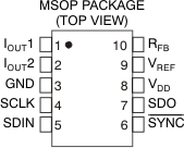
5 Pin Configuration and Functions
DGS Package
10-Pin VSSOP
Top View

Pin Functions
| PIN | TYPE | DESCRIPTION | |
|---|---|---|---|
| NO. | NAME | ||
| 1 | IOUT1 | O | DAC Current Output |
| 2 | IOUT2 | O | DAC Analog Ground. This pin is normally tied to the analog ground of the system. |
| 3 | GND | G | Ground pin. |
| 4 | SCLK | I | Serial Clock Input. By default, data is clocked into the input shift register on the falling edge of the serial clock input. Alternatively, by means of the serial control bits, the device may be configured such that data is clocked into the shift register on the rising edge of SCLK. |
| 5 | SDIN | I | Serial Data Input. Data is clocked into the 16-bit input register on the active edge of the serial clock input. By default, on power-up, data is clocked into the shift register on the falling edge of SCLK. The control bits allow the user to change the active edge to the rising edge. |
| 6 | SYNC | I | Active Low Control Input. This is the frame synchronization signal for the input data. When SYNC goes low, it powers on the SCLK and DIN buffers, and the input shift register is enabled. Data is loaded to the shift register on the active edge of the following clocks (power-on default is falling clock edge). In stand-alone mode, the serial interface counts the clocks and data is latched to the shift register on the 16th active clock edge. |
| 7 | SDO | O | Serial Data Output. This allows a number of parts to be daisy-chained. By default, data is clocked into the shift register on the falling edge and out via SDO on the rising edge of SCLK. Data will always be clocked out on the alternate edge to loading data to the shift register. Writing the Readback control word to the shift register makes the DAC register contents available for readback on the SDO pin, clocked out on the opposite edges to the active clock edge. |
| 8 | VDD | I | Positive Power Supply Input. These parts can be operated from a supply of 2.7 V to 5.5 V. |
| 9 | VREF | I | DAC Reference Voltage Input |
| 10 | RFB | O | DAC Feedback Resistor pin. Establish voltage output for the DAC by connecting to external amplifier output. |