ZHCSHU4E April   2005  – March 2018 DAC7811

PRODUCTION DATA.  

  1. 特性
  2. 应用
  3. 说明
    1.     Device Images
      1.      框图
  4. 修订历史记录
  5. Pin Configuration and Functions
    1.     Pin Functions
  6. Specifications
    1. 6.1 Absolute Maximum Ratings
    2. 6.2 ESD Ratings
    3. 6.3 Recommended Operating Conditions
    4. 6.4 Thermal Information
    5. 6.5 Electrical Characteristics
    6. 6.6 Typical Characteristics: VDD = 5 V
    7. 6.7 Typical Characteristics: VDD = 2.7 V
  7. Detailed Description
    1. 7.1 Overview
    2. 7.2 Functional Block Diagram
    3. 7.3 Feature Description
    4. 7.4 Device Functional Modes
      1. 7.4.1 Serial Interface
      2. 7.4.2 Input Shift Register
      3. 7.4.3 SYNC Interrupt (Stand-Alone Mode)
      4. 7.4.4 Daisy-Chain
      5. 7.4.5 Control Bits C3 to C0
  8. Application and Implementation
    1. 8.1 Application Information
      1. 8.1.1 Unipolar Operation Using DAC7811
      2. 8.1.2 Bipolar Operation Using the DAC7811
      3. 8.1.3 Stability Circuit
      4. 8.1.4 Amplifier Selection
      5. 8.1.5 Programmable Current Source Circuit
    2. 8.2 Typical Application
      1. 8.2.1 Single Supply Unipolar Multiplying DAC
        1. 8.2.1.1 Design Requirements
        2. 8.2.1.2 Detailed Design Procedure
        3. 8.2.1.3 Application Curve
  9. Power Supply Recommendations
  10. 10Layout
    1. 10.1 Layout Guidelines
    2. 10.2 Layout Example
  11. 11器件和文档支持
    1. 11.1 文档支持
      1. 11.1.1 相关文档
    2. 11.2 接收文档更新通知
    3. 11.3 社区资源
    4. 11.4 商标
    5. 11.5 静电放电警告
    6. 11.6 Glossary
  12. 12机械、封装和可订购信息

封装选项

机械数据 (封装 | 引脚)
散热焊盘机械数据 (封装 | 引脚)
订购信息

Stability Circuit

For a current-to-voltage design (see Figure 30), the DAC7811 current output (IOUT) and the connection with the inverting node of the op amp should be as short as possible and according to correct printed circuit board (PCB) layout design practices. For each code change, there is a step function. If the gain bandwidth product (GBP) of the op amp is limited and parasitic capacitance is excessive at the inverting node, then gain peaking is possible. Therefore, for circuit stability, a compensation capacitor C1 (1pF to 5pF typ) can be added to the design, as shown in Figure 30.
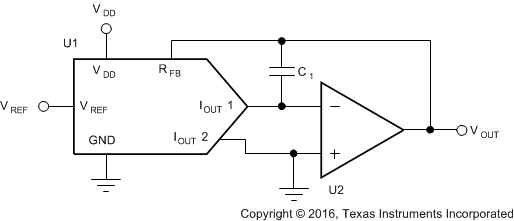
DAC7811 ai_gain_bas337.gifFigure 30. Gain Peaking Prevention Circuit With Compensation Capacitor