SLLS853F August 2007 – January 2015 DAC5682Z
PRODUCTION DATA.
- 1 Features
- 2 Applications
- 3 Description
- 4 Revision History
- 5 Description (continued)
- 6 Pin Configuration and Functions
- 7 Specifications
-
8 Detailed Description
- 8.1 Overview
- 8.2 Functional Block Diagram
- 8.3
Feature Description
- 8.3.1 FIR Filters
- 8.3.2 Coarse Mixers: CMIX0 and CMIX1
- 8.3.3 Clock Inputs
- 8.3.4 LVDS Data Interfacing
- 8.3.5 LVDS Inputs
- 8.3.6 LVDS SYNCP/N Operation
- 8.3.7 DLL Operation
- 8.3.8 CMOS Digital Inputs
- 8.3.9 Reference Operation
- 8.3.10 DAC Transfer Function
- 8.3.11 DAC Output SINC Response
- 8.3.12 Analog Current Outputs
- 8.3.13 Designing the PLL Loop Filter
- 8.3.14 Test Methodology
- 8.4 Device Functional Modes
- 8.5 Programming
- 8.6
Register Maps
- 8.6.1 Register Name: STATUS0 - Address: 0x00, Default = 0x03
- 8.6.2 Register Name: CONFIG1 - Address: 0x01, Default = 0x10
- 8.6.3 Register Name: CONFIG2 - Address: 0x02, Default = 0xC0
- 8.6.4 Register Name: CONFIG3 - Address: 0x03, Default = 0x70
- 8.6.5 Register Name: STATUS4 - Address: 0x04, Default = 0x00
- 8.6.6 Register Name: CONFIG5 - Address: 0x05, Default = 0x00
- 8.6.7 Register Name: CONFIG6 - Address: 0x06, Default = 0x0C
- 8.6.8 Register Name: CONFIG7 - Address: 0x07, Default = 0xFF
- 8.6.9 Register Name: CONFIG8 - Address: 0x08, Default = 0x00
- 8.6.10 Register Name: CONFIG9 - Address: 0x09, Default = 0x00
- 8.6.11 Register Name: CONFIG10 - Address: 0x0A, Default = 0x00
- 8.6.12 Register Name: CONFIG11 - Address: 0x0B, Default = 0x00
- 8.6.13 Register Name: CONFIG12 - Address: 0x0C, Default = 0x00
- 8.6.14 Register Name: CONFIG13 - Address: 0x0D, Default = 0x00
- 8.6.15 Register Name: CONFIG14 - Address: 0x0E, Default = 0x00
- 8.6.16 Register Name: CONFIG15 - Address: 0x0F, Default = 0x00
- 9 Application and Implementation
- 10Power Supply Recommendations
- 11Layout
- 12Device and Documentation Support
- 13Mechanical, Packaging, and Orderable Information
封装选项
请参考 PDF 数据表获取器件具体的封装图。
机械数据 (封装 | 引脚)
- RGC|64
散热焊盘机械数据 (封装 | 引脚)
- RGC|64
订购信息
11 Layout
11.1 Layout Guidelines
The DAC5682Z EVM layout should be used as a reference for the layout to obtain the best performance. A sample layout is shown in Figure 53. Some important layout recommendations are:
- Use a single ground plane. Keep the digital and analog signals on distinct separate sections of the board. This may be virtually divided down the middle of the device package when doing placement and layout.
- Keep the analog outputs as far away from the switching clocks and digital signals as possible. This will keep coupling from the digital circuits to the analog outputs to a minimum.
- Decoupling caps should be kept close to the power pins of the device.
11.2 Layout Example
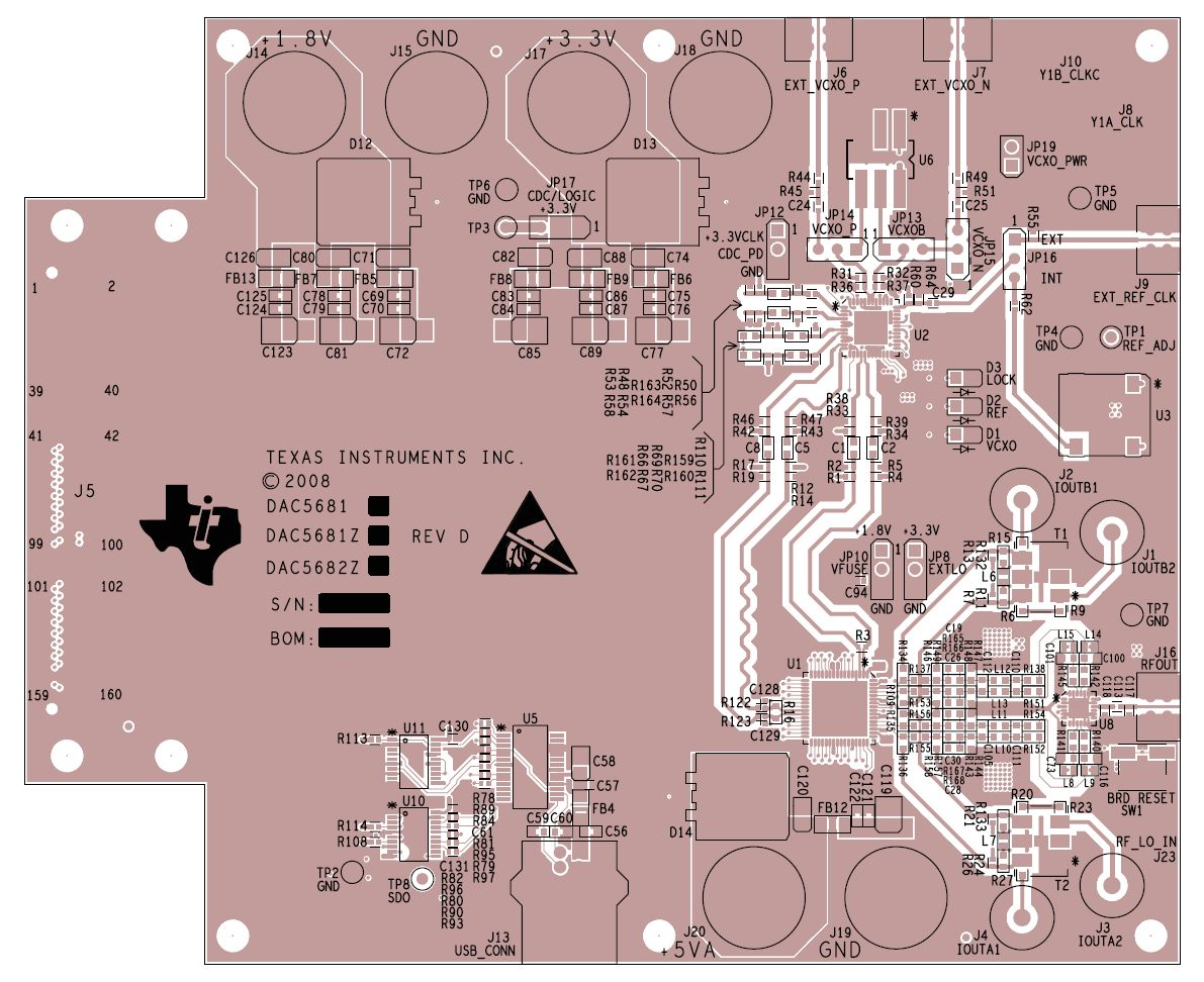 Figure 53. Top Layer of DAC5682zEVM Layout