SLLS853F August 2007 – January 2015 DAC5682Z
PRODUCTION DATA.
- 1 Features
- 2 Applications
- 3 Description
- 4 Revision History
- 5 Description (continued)
- 6 Pin Configuration and Functions
- 7 Specifications
-
8 Detailed Description
- 8.1 Overview
- 8.2 Functional Block Diagram
- 8.3
Feature Description
- 8.3.1 FIR Filters
- 8.3.2 Coarse Mixers: CMIX0 and CMIX1
- 8.3.3 Clock Inputs
- 8.3.4 LVDS Data Interfacing
- 8.3.5 LVDS Inputs
- 8.3.6 LVDS SYNCP/N Operation
- 8.3.7 DLL Operation
- 8.3.8 CMOS Digital Inputs
- 8.3.9 Reference Operation
- 8.3.10 DAC Transfer Function
- 8.3.11 DAC Output SINC Response
- 8.3.12 Analog Current Outputs
- 8.3.13 Designing the PLL Loop Filter
- 8.3.14 Test Methodology
- 8.4 Device Functional Modes
- 8.5 Programming
- 8.6
Register Maps
- 8.6.1 Register Name: STATUS0 - Address: 0x00, Default = 0x03
- 8.6.2 Register Name: CONFIG1 - Address: 0x01, Default = 0x10
- 8.6.3 Register Name: CONFIG2 - Address: 0x02, Default = 0xC0
- 8.6.4 Register Name: CONFIG3 - Address: 0x03, Default = 0x70
- 8.6.5 Register Name: STATUS4 - Address: 0x04, Default = 0x00
- 8.6.6 Register Name: CONFIG5 - Address: 0x05, Default = 0x00
- 8.6.7 Register Name: CONFIG6 - Address: 0x06, Default = 0x0C
- 8.6.8 Register Name: CONFIG7 - Address: 0x07, Default = 0xFF
- 8.6.9 Register Name: CONFIG8 - Address: 0x08, Default = 0x00
- 8.6.10 Register Name: CONFIG9 - Address: 0x09, Default = 0x00
- 8.6.11 Register Name: CONFIG10 - Address: 0x0A, Default = 0x00
- 8.6.12 Register Name: CONFIG11 - Address: 0x0B, Default = 0x00
- 8.6.13 Register Name: CONFIG12 - Address: 0x0C, Default = 0x00
- 8.6.14 Register Name: CONFIG13 - Address: 0x0D, Default = 0x00
- 8.6.15 Register Name: CONFIG14 - Address: 0x0E, Default = 0x00
- 8.6.16 Register Name: CONFIG15 - Address: 0x0F, Default = 0x00
- 9 Application and Implementation
- 10Power Supply Recommendations
- 11Layout
- 12Device and Documentation Support
- 13Mechanical, Packaging, and Orderable Information
封装选项
请参考 PDF 数据表获取器件具体的封装图。
机械数据 (封装 | 引脚)
- RGC|64
散热焊盘机械数据 (封装 | 引脚)
- RGC|64
订购信息
8 Detailed Description
8.1 Overview
The DAC5682Z is a dual-channel 16-bit 1.0 GSPS DAC with wideband LVDS data input, integrated 2x/4x interpolation filters, onboard clock multiplier and internal voltage reference. The DAC5682Z offers superior linearity, noise, crosstalk, and PLL phase noise performance.
The DAC5682Z integrates a wideband LVDS port with on-chip termination. Full-rate input data can be transferred to a single DAC channel, or half-rate and 1/4-rate input data can be interpolated by onboard 2x or 4x FIR filters. Each interpolation FIR is configurable in either Low-Pass or High-Pass mode, allowing selection of a higher order output spectral image. An on-chip delay lock loop (DLL) simplifies LVDS interfacing by providing skew control for the LVDS input data clock.
The DAC5682Z allows both complex or real output. An optional Fs/4 coarse mixer in complex mode provides coarse frequency upconversion and the dual DAC output produces a complex Hilbert Transform pair. An external RF quadrature modulator then performs the final single sideband up-conversion. The interpolation filters and complex coarse mixers efficiently provide frequency plan flexibility while enabling higher output DAC rates to simplify image rejection filtering.
8.2 Functional Block Diagram
8.3 Feature Description
8.3.1 FIR Filters
Figure 24 shows the magnitude spectrum response for the identical 47-tap FIR0 and FIR1 filters. The transition band is from 0.4 to 0.6 × FIN (the input data rate for the FIR filter) with <0.002 dB of pass-band ripple and approximately 76 dB of stop-band attenuation. Figure 25 shows the region from 0.35 to 0.45 × FIN – up to 0.44x FIN there is less than 0.4 dB attenuation. The composite spectrum for x4 interpolation mode, the cascaded response of FIR0 and FIR1, is shown in Figure 26. The filter taps for both FIR0 and FIR1 are listed in Table 1.
 Figure 26. Magnitude Composite Spectrum for 4x Interpolation Mode
Table 1. FIR0 and FIR1 Digital Filter Taps
| TAP NO. | COEFF | TAP NO. | COEFF |
|---|---|---|---|
| 1, 47 | –5 | 2, 46 | 0 |
| 3, 45 | 18 | 4, 44 | 0 |
| 5, 43 | –42 | 6, 42 | 0 |
| 7, 41 | 85 | 8, 40 | 0 |
| 9, 39 | –158 | 10, 38 | 0 |
| 11, 37 | 272 | 12, 36 | 0 |
| 13, 35 | –444 | 14, 34 | 0 |
| 15, 33 | 704 | 16, 32 | 0 |
| 17, 31 | –1106 | 18, 30 | 0 |
| 19, 29 | 1795 | 20, 28 | 0 |
| 21, 27 | –3295 | 22, 26 | 0 |
| 23, 25 | 10368 | — | — |
| 24 | 16384 | — | — |
8.3.2 Coarse Mixers: CMIX0 and CMIX1
The DAC5682Z has two coarse mixer (CMIX) blocks: CMIX0 follows FIR0 and CMIX1 follows FIR1. (See Figure 27) Each CMIX block provides mixing capability of fixed frequencies Fs/2 (real) or ±Fs/4 (complex) with respect to the output frequency of the preceding FIR block. Because FIR0 and CMIX0 are only used in x4 interpolation modes, the output is half-rate relative to the DAC output frequency. Therefore, an ±Fs/4 mixing sequence results in ±FDAC/8 frequency shift at the DAC output.
Table 2. CMIX0 Mixer Sequences
| Mode | CMIX0_mode(1) | CMIX0_mode(0) | MIXING SEQUENCE |
|---|---|---|---|
| Normal (Low Pass, No Mixing) |
0 | 0 | FIR0A = { +A, +A , +A, +A } FIR0B = { +B, +B , +B, +B } |
| High Pass | 0 | 1 | FIR0A = { +A, –A , +A, –A } FIR0B = { +B, –B , +B, –B } |
| +FDAC /8 (+Fs/4) | 1 | 0 | FIR0A = { +A, –B , –A, +B } FIR0B = { +B, +A , –B, –A } |
| –FDAC /8 (–Fs/4) | 1 | 1 | FIR0A = { +A, +B , –A, –B } FIR0B = { +B, –A , –B, +A } |
Table 3. CMIX1 Mixer Sequences
| Mode | CMIX1_mode(1) | CMIX1_mode(0) | MIXING SEQUENCE |
|---|---|---|---|
| Normal (Low Pass, No Mixing) |
0 | 0 | DACA = { +A, +A , +A, +A } DACB = { +B, +B , +B, +B } |
| High Pass (Fs/2) | 0 | 1 | DACA = { +A, –A , +A, –A } DACB = { +B, –B , +B, –B } |
| +FDAC /4 | 1 | 0 | DACA = { +A, –B , –A, +B } DACB = { +B, +A , –B, –A } |
| –FDAC /4 | 1 | 1 | DACA = { +A, +B , –A, –B } DACB = { +B, –A , –B, +A } |
 Figure 27. CMIX0 and CMIX1 Coarse Mixers Block Diagram
8.3.3 Clock Inputs
Figure 28 shows an equivalent circuit for the LVDS data input clock (DCLKP/N).
 Figure 28. DCLKP/N Equivalent Input Circuit
Figure 29 shows an equivalent circuit for the DAC input clock (CLKIN/C).
 Figure 29. CLKIN/C Equivalent Input Circuit
Figure 30 shows the preferred configuration for driving the CLKIN/CLKINC input clock with a differential ECL/PECL source.
8.3.4 LVDS Data Interfacing
Interfacing very high-speed LVDS data and clocks presents a big challenge to system designers as they have unique constraints and are often implemented with specialized circuits to increase bandwidth. One such specialized LVDS circuit used in many FPGAs and ASICs is a SERializer-DESerializer (SERDES) block. For interfacing to the DAC5682Z, only the SERializer functionality of the SERDES block is required. SERDES drivers accept lower rate parallel input data and output a serial stream using a shift register at a frequency multiple of the data bit width. For example, a 4-bit SERDES block can accept parallel 4-bit input data at 250 MSPS and output serial data 1000 MSPS.
External clock distribution for FPGA and ASIC SERDES drivers often have a chip-to-chip system constraint of a limited input clock frequency compared to the desired LVDS data rate. In this case, an internal clock multiplying PLL is often used in the FPGA or ASIC to drive the high-rate SERDES outputs. Due to this possible system clocking constraint, the DAC5682Z accommodates a scheme where a toggling LVDS SERDES data bit can provide a “data driven” half-rate clock (DCLK) from the data source. A DLL onboard the DAC is used to shift the DCLK edges relative to LVDS data to maintain internal setup and hold timing.
To increase bandwidth of a single 16-bit input bus, the DAC5682Z assumes Double Data Rate (DDR) style interfacing of data relative to the half-rate DCLK. Refer to Figure 31 and Figure 32 for an example implementation using FPGA-based LVDS data and clock interfaces to drive the DAC5682Z. In this example, an assumed system constraint is that the FPGA can only receive a 250 MHz maximum input clock while the desired DAC clock is 1000 MHz. A clock distribution chip such as the CDCM7005 or the CDCE62005 is useful in this case to provide frequency and phase locked clocks at 250 MHz and 1000 MHz.
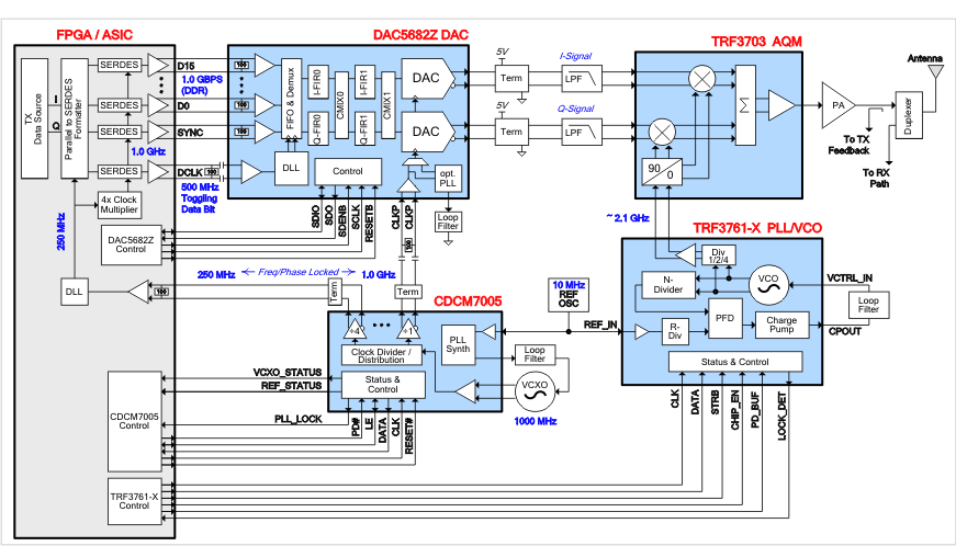 Figure 31. Example Direct Conversion System Diagram
From the example provided by Figure 32, driving LVDS data into the DAC using SERDES blocks requires a parallel load of 4 consecutive data samples to shift registers. Color is used in the figure to indicate how data and clocks flow from the FPGA to the DAC5682Z. The figure also shows the use of the SYNCP/N input, which along with DCLK, requires 18 individual SERDES data blocks to drive the input data FIFO of the DAC that provides an elastic buffer to the DAC5682Z digital processing chain.
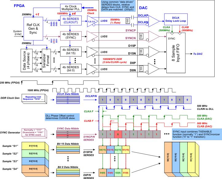 Figure 32. Example FPGA-Based LVDS Data Flow to DAC
8.3.5 LVDS Inputs
The D[15:0]P/N and SYNCP/N LVDS pairs have the input configuration shown in Figure 33. Figure 34 shows the typical input levels and common-mode voltage used to drive these inputs.
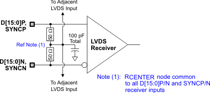 Figure 33. D[15:0]P/N and SYNCP/N LVDS Input Configuration
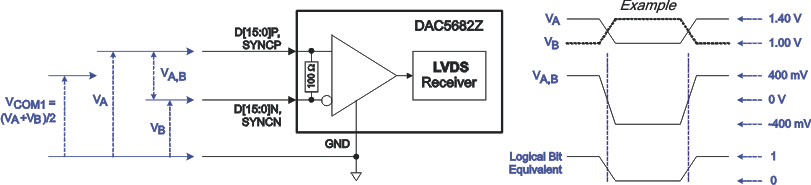
Table 4. Example LVDS Data Input Levels
| APPLIED VOLTAGES | RESULTING DEFERENTIAL VOLTAGE | RESULTING COMMON-MODE VOLTAGE | LOGICAL BIT BINARY EQUIVALENT | |
|---|---|---|---|---|
| VA | VB | VA,B | VCOM1 | |
| 1.4 V | 1.0 V | 400 mV | 1.2 V | 1 |
| 1.0 V | 1.4 V | –400 mV | 0 | |
| 1.2 V | 0.8 V | 400 mV | 1.0 V | 1 |
| 0.8 V | 1.2 V | –400 mV | 0 | |
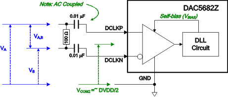
Figure 35 shows the DCLKP/N LVDS clock input levels. Unlike the D[15:0]P/N and SYNCP/N LVDS pairs, the DCLKP/N pair does not have an internal resistor and the common-mode voltage is self-biased to approximately DVDD/2 in order to optimize the operation of the DLL circuit. For proper external termination a 100-Ω resistor needs to be connected across the LVDS clock source lines followed by series 0.01-μF capacitors connected to each of the DCLKP and DCLKN pairs. For best performance, the resistor and capacitors should be placed as close as possible to these pins.
8.3.6 LVDS SYNCP/N Operation
The SYNCP/N LVDS input control functions as a combination of Transmit Enable (TXENABLE) and Synchronization trigger. If SYNCP is low, the transmit chain is disabled so input data from the FIFO is ignored while zero amplitude samples are inserted into the data path. If SYNCP is raised from low to high, a synchronization event occurs with behavior defined by individual control bits in registers CONFIG1 and CONFIG5. The SYNCP/N control is sampled and input into the FIFO along with the other LVDS data to maintain timing alignment with the data bus. Refer to Figure 32.
The software_sync_sel and software_sync controls in CONFIG3 provide a substitute for external SYNCP/N control; however, because the serial interface is used, no timing control is provided with respect to the DAC clock.
8.3.7 DLL Operation
The DAC5682Z provides a digital delay lock loop (DLL) to skew the LVDS data clock (DCLK) relative to the data bits, D[15:0] and SYNC, in order to maintain proper setup and hold timing. Because the DLL operates closed-loop, it requires a stable DCLK to maintain delay lock. Refer to the description of DLL_ifixed(2:0) and DLL_delay(3:0) control bits in the CONFIG10 register. Prior to initializing the DLL, the DLL_ifixed value should be programmed to match the expected DCLK frequency range. To initialize the DLL, refer to the DLL_Restart programming bit in the CONFIG8 register. After initialization, the status of the DLL can be verified by reading the DLL_Lock bit from STATUS0. See Recommended Start-up Sequence below.
8.3.8 CMOS Digital Inputs
Figure 36 shows a schematic of the equivalent CMOS digital inputs of the DAC5682Z. SDIO and SCLK have pulldown resistors while RESETB and SDENB have pullup resistors internal the DAC5682Z. See the specification table for logic thresholds. The pullup and pulldown circuitry is approximately equivalent to 100kΩ.
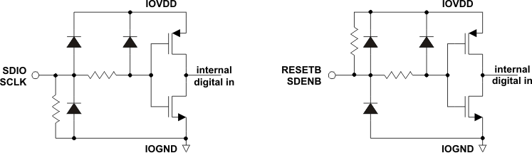 Figure 36. CMOS/TTL Digital Equivalent Input
8.3.9 Reference Operation
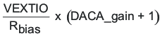
The DAC5682Z uses a bandgap reference and control amplifier for biasing the full-scale output current. The full-scale output current is set by applying an external resistor RBIAS to pin BIASJ. The bias current IBIAS through resistor RBIAS is defined by the on-chip bandgap reference voltage and control amplifier. The default full-scale output current equals 16 times this bias current and can thus be expressed as:
Each DAC has a 4-bit independent coarse gain control via DACA_gain(3:0) and DACB_gain(3:0) in the CONFIG7 register. Using gain control, the IOUTFS can be expressed as:
where VEXTIO is the voltage at terminal EXTIO. The bandgap reference voltage delivers an accurate voltage of 1.2 V. This reference is active when terminal EXTLO is connected to AGND. An external decoupling capacitor CEXT of 0.1 μF should be connected externally to terminal EXTIO for compensation. The bandgap reference can additionally be used for external reference operation. In that case, an external buffer with high impedance input should be applied in order to limit the bandgap load current to a maximum of 100 nA. The internal reference can be disabled and overridden by an external reference by connecting EXTLO to AVDD. Capacitor CEXT may hence be omitted. Terminal EXTIO thus serves as either input or output node.
The full-scale output current can be adjusted from 20 mA down to 2 mA by varying resistor RBIAS or changing the externally applied reference voltage. The internal control amplifier has a wide input range, supporting the full-scale output current range of 20 dB.
8.3.10 DAC Transfer Function
The CMOS DAC’s consist of a segmented array of NMOS current sinks, capable of sinking a full-scale output current up to 20 mA. Differential current switches direct the current to either one of the complementary output nodes IOUT1 or IOUT2. (DACA = IOUTA1 or IOUTA2 and DACB = IOUTB1 or IOUTB2.) Complementary output currents enable differential operation, thus canceling out common mode noise sources (digital feed-through, on-chip and PCB noise), dc offsets, even order distortion components, and increasing signal output power by a factor of two.
The full-scale output current is set using external resistor RBIAS in combination with an on-chip bandgap voltage reference source (+1.2 V) and control amplifier. Current IBIAS through resistor RBIAS is mirrored internally to provide a maximum full-scale output current equal to 16 times IBIAS.
The relation between IOUT1 and IOUT2 can be expressed as:
We will denote current flowing into a node as – current and current flowing out of a node as + current. Because the output stage is a current sink the current can only flow from AVDD into the IOUT1 and IOUT2 pins. The output current flow in each pin driving a resistive load can be expressed as:
where CODE is the decimal representation of the DAC data input word.
For the case where IOUT1 and IOUT2 drive resistor loads RL directly, this translates into single ended voltages at IOUT1 and IOUT2:
Assuming that the data is full scale (65536 in offset binary notation) and the RL is 25 Ω, the differential voltage between pins IOUT1 and IOUT2 can be expressed as:
Do not exceed the compliance voltages at node IOUT1 and IOUT2, which would lead to increased signal distortion.
8.3.11 DAC Output SINC Response
Due to sampled nature of a high-speed DAC, the well known sin(x)/x (or SINC) response can significantly attenuate higher frequency output signals. See the Figure 37 which shows the unitized SINC attenuation roll-off with respect to the final DAC sample rate in 4 Nyquist zones. For example, if the final DAC sample rate FS = 1.0 GSPS, then a tone at 440MHz is attenuated by 3.0dB. Although the SINC response can create challenges in frequency planning, one side benefit is the natural attenuation of Nyquist images. The increased over-sampling ratio of the input data provided by the 2x and 4x digital interpolation modes of the DAC5682Z improve the SINC roll-off (droop) within the band of interest of the original signal.
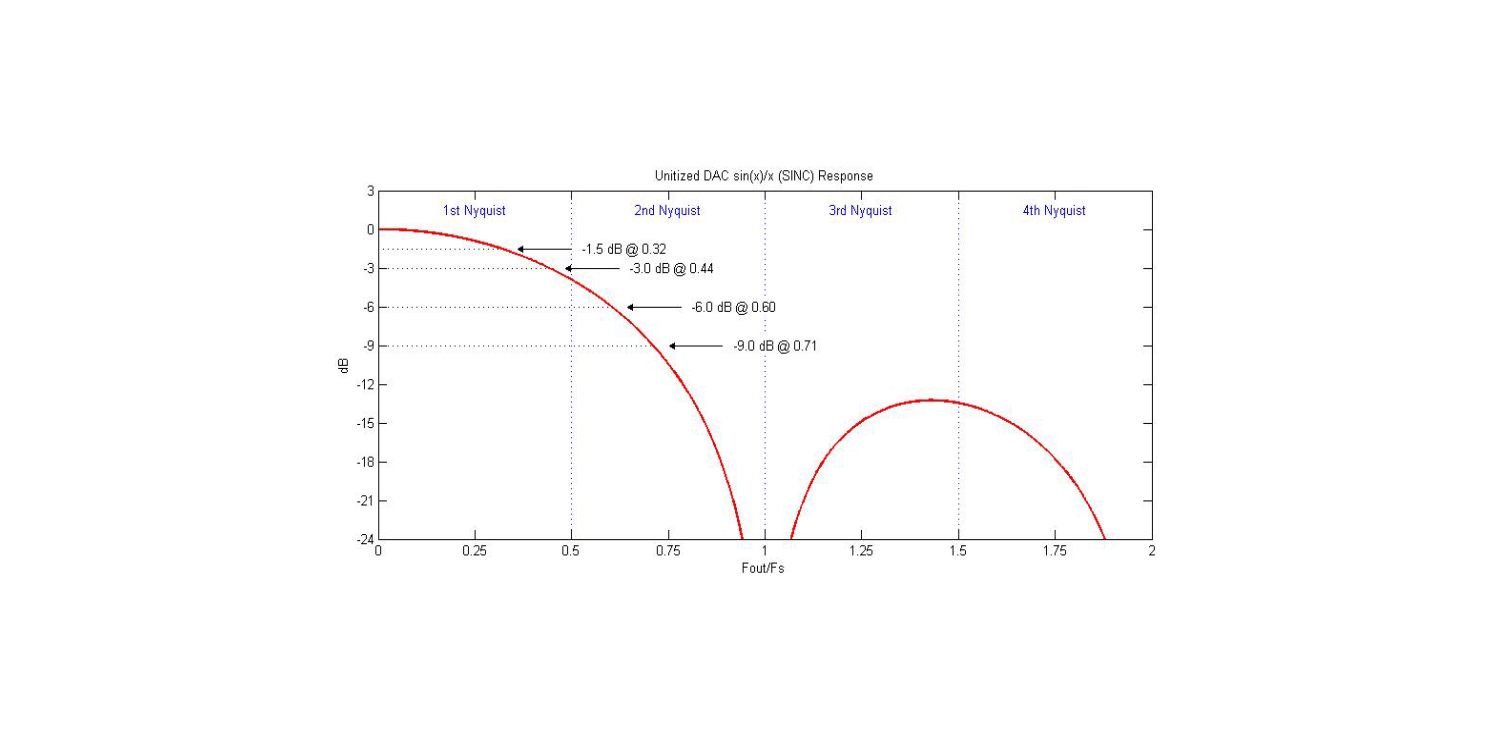 Figure 37. Unitized DAC sin(x)/x (SINC) Response
8.3.12 Analog Current Outputs
Figure 38 shows a simplified schematic of the current source array output with corresponding switches in a current sink configuration. Differential switches direct the current into either the positive output node, IOUT1, or its complement, IOUT2, then through the individual NMOS current sources. The output impedance is determined by the stack of the current sources and differential switches, and is typically >300 kΩ in parallel with an output capacitance of 5 pF.
The external output resistors are referred to an external ground. The minimum output compliance at nodes IOUT1 and IOUT2 is limited to AVDD – 0.5 V, determined by the CMOS process. Beyond this value, transistor breakdown may occur resulting in reduced reliability of the DAC5682Z device. The maximum output compliance voltage at nodes IOUT1 and IOUT2 equals AVDD + 0.5 V. Exceeding the minimum output compliance voltage adversely affects distortion performance and integral non-linearity. The optimum distortion performance for a single-ended or differential output is achieved when the maximum full-scale signal at IOUT1 and IOUT2 does not exceed 0.5 V.
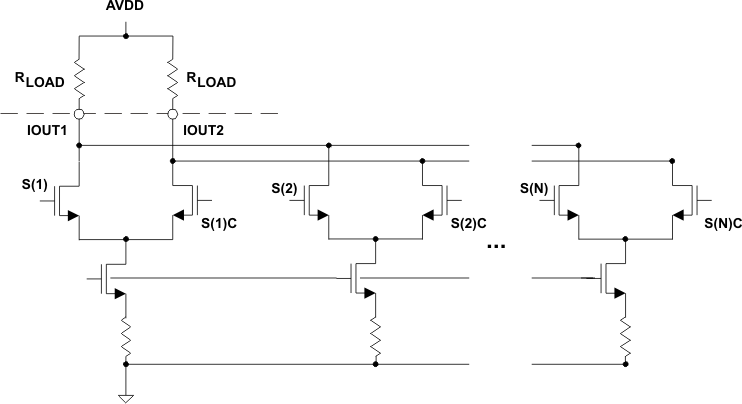 Figure 38. Equivalent Analog Current Output
The DAC5682Z can be easily configured to drive a doubly terminated 50Ω cable using a properly selected RF transformer. Figure 39 and Figure 40 show the 50Ω doubly terminated transformer configuration with 1:1 and 4:1 impedance ratio, respectively. The center tap of the primary input of the transformer must be connected to AVDD to enable a dc current flow. Applying a 20-mA full-scale output current would lead to a 0.5 VPP for a 1:1 transformer and a 1 VPP output for a 4:1 transformer. The low dc-impedance between IOUT1 or IOUT2 and the transformer center tap sets the center of the ac-signal at AVDD, so the 1 VPP output for the 4:1 transformer results in an output between AVDD + 0.5 V and AVDD – 0.5 V.
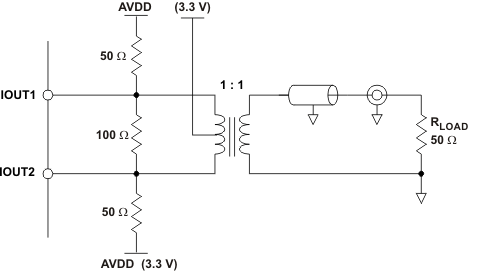 Figure 39. Driving a Doubly Terminated 50-Ω Cable Using a 1:1 Impedance Ratio Transformer
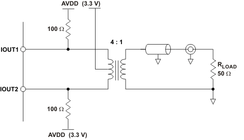 Figure 40. Driving a Doubly Terminated 50-Ω Cable Using a 4:1 Impedance Ratio Transformer
8.3.13 Designing the PLL Loop Filter
To minimize phase noise given for a given fDAC and M/N, the values of PLL_gain and PLL_range are selected so that GVCO is minimized and within the MIN and MAX frequency for a given setting.
The external loop filter components C1, C2, and R1 are set by the GVCO, M/N, the loop phase margin φd and the loop bandwidth ωd. Except for applications where abrupt clock frequency changes require a fast PLL lock time, it is suggested that φd be set to at least 80 degrees for stable locking and suppression of the phase noise side lobes. Phase margins of 60 degrees or less can be sensitive to board layout and decoupling details.
See Figure 41, the recommend external loop filter topology. C1, C2, and R1 are calculated by the following equations:
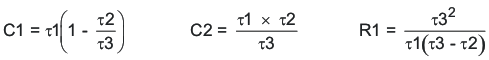
where,

charge pump current: iqp = 1 mA
vco gain: KVCO = 2π × GVCO rad/V
PFD Frequency: ωd ≤160 MHz
phase detector gain: Kd = iqp ÷ (2 × π × M) A/rad
An Excel spreadsheet is available from Texas Instruments for automatically calculating the values for C1, R1 and C2 in the DAC5682 LPF Caluclator (SLAC169).
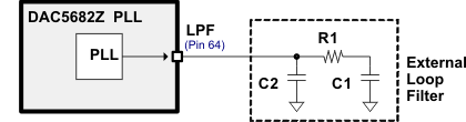 Figure 41. Recommended External Loop Filter Topology
8.3.14 Test Methodology
Typical AC specifications were characterized with the DAC5682ZEVM using the test configuration shown in Figure 42. A sinusoidal master clock frequency is generated by an HP8665B signal generator and into a splitter. One output drives an Agilent 8133A pulse generator, and the other drives the CDCM7005 clock driver. The 8133A converts the sinusoidal frequency into a square wave output clock and drives an Agilent ParBERT 81250A pattern-generator clock. On the EVM, the DAC5682Z CLKIN/C input clock is driven by an CDCM7005 clock distribution chip that is configured to simply buffer the external 8665B clock or divide it down for PLL test configurations.
The DAC5682Z output is characterized with a Rohde and Schwarz FSU spectrum analyzer. For WCDMA signal characterization, it is important to use a spectrum analyzer with high IP3 and noise subtraction capability so that the spectrum analyzer does not limit the ACPR measurement. For all specifications, both DACA and DACB are measured and the lowest value used as the specification.
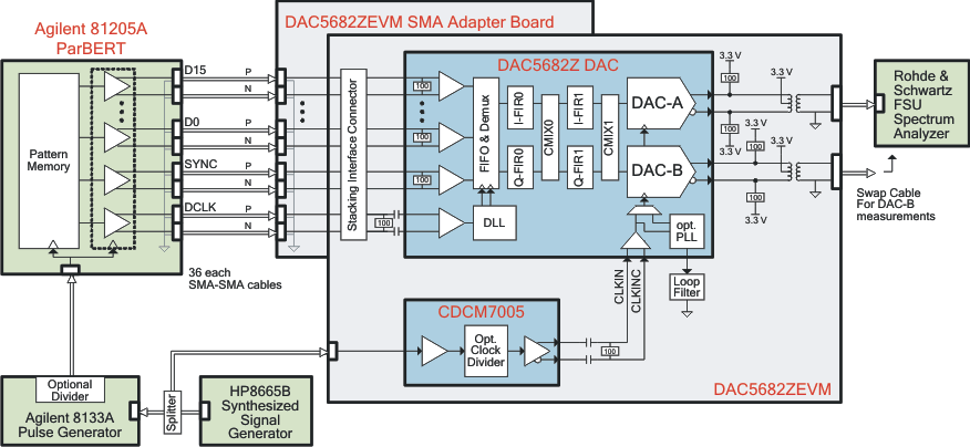 Figure 42. DAC5682Z Test Configuration for Normal Clock Mode
8.4 Device Functional Modes
8.4.1 Dual-Channel Real Upconversion
The DAC5682Z can be used in a dual channel mode with real upconversion by mixing with a 1, –1, … sequence in the signal chain to invert the spectrum. This mixing mode maintains isolation of the A and B channels. The two points of mixing, CMIX0 and CMIX1, follow each FIR filter. The mixing modes for each CMIX block are controlled by CMIX0_mode(1:0) and CMIX1(1:0) in register CONFIG2. The wide bandwidths of both FIR0 and FIR1 (40% passband) provide options for setting the frequency ranges listed in Table 5. With the High Pass (2x2 HP mode), High Pass/Low Pass (2X4 HP/LP mode) and Low Pass/High Pass (2X4 LP/HP mode) settings, the upconverted signal is spectrally inverted.
Table 5. Dual-Channel Real Upconversion Options
| MODE NAME | INTERP. FACTOR | FIR0, CMIX0 MODE | FIR1, CMIX1 MODE | INPUT FREQUENCY(1) | OUTPUT FREQUENCY(1) | SIGNAL BANDWIDTH(1) | SPECTRUM INVERTED? |
|---|---|---|---|---|---|---|---|
| 2X2 | X2 | -- | LP | 0.0 to 0.4 × fDATA | 0.0 to 0.4 × fDATA | 0.4 × fDATA | No |
| 2X2 HP | X2 | -- | HP | 0.0 to 0.4 × fDATA | 0.6 to 1.0 × fDATA | 0.4 × fDATA | Yes |
| 1X4 | X4 | LP | LP | 0.0 to 0.4 × fDATA | 0.0 to 0.4 × fDATA | 0.4 × fDATA | No |
| 2X4 | X4 | LP | LP | 0.0 to 0.4 × fDATA | 0.0 to 0.4 × fDATA | 0.4 × fDATA | No |
| 2X4 HP/LP | X4 | HP | LP | 0.2 to 0.4 × fDATA | 0.6 to 0.8 × fDATA | 0.2 × fDATA | Yes |
| 2X4 HP/HP | X4 | HP | HP | 0.2 to 0.4 × fDATA | 1.2 to 1.4 × fDATA | 0.2 × fDATA | No |
| 2X4 LP/HP | X4 | LP | HP | 0.0 to 0.4 × fDATA | 1.6 to 2.0 × fDATA | 0.4 × fDATA | Yes |
8.4.2 Clock and Data Modes
There are two modes of operation to drive the internal clocks on the DAC5682Z. Timing diagrams for both modes are shown in Figure 43. EXTERNAL CLOCK MODE accepts an external full-rate clock input on the CLKIN/CLKINC pins to drive the DACs and final logic stages while distributing an internally divided down clock for lower speed logic such as the interpolating FIRs. PLL CLOCK MODE uses an internal clock multiplying PLL to derive the full-rate clock from an external lower rate reference frequency on the CLKIN/CLKINC pins. In both modes, an LVDS half-rate data clock (DCLKP/DCLKN) is provided by the user and is typically generated by a toggling data bit to maintain LVDS data to DCLK timing alignment. LVDS data relative to DCLK is input using Double Data Rate (DDR) switching using both rising and falling edges as shown in the both figures below. The CONFIG10 register contains user controlled settings for the DLL to adjust for the DCLK input frequency and various tSKEW timing offsets between the LVDS data and DCLK. The CDCM7005 and CDCE62005 from Texas Instruments are recommended for providing phase aligned clocks at different frequencies for device-to-device clock distribution and multiple DAC synchronization.
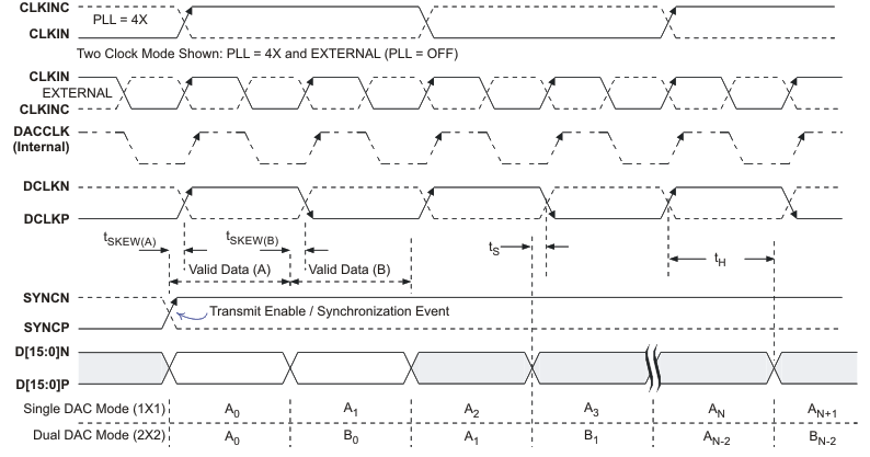 Figure 43. Clock and Data Timing Diagram
8.4.3 PLL Clock Mode
In PLL Clock Mode, the user provides an external reference clock to the CLKIN/C input pins. Refer to Figure 44. An internal clock multiplying PLL uses the lower-rate reference clock to generate a high-rate clock for the DAC. This function is very useful when a high-rate clock is not already available at the system level; however, the internal VCO phase noise in PLL Clock Mode may degrade the quality of the DAC output signal when compared to an external low jitter clock source.
The internal PLL has a type four phase-frequency detector (PFD) comparing the CLKIN/C reference clock with a feedback clock to drive a charge pump controlling the VCO operating voltage and maintaining synchronization between the two clocks. An external low-pass filter is required to control the loop response of the PLL. See Designing the PLL Loop Filter for the filter setting calculations. This is the only mode where the LPF filter applies.
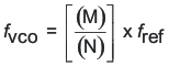
The input reference clock N-Divider is selected by CONFIG9 PLL_n(2:0) for values of ÷1, ÷2, ÷4 or ÷8. The VCO feedback clock M-Divider is selected by CONFIG9 PLL_m(4:0) for values of ÷1, ÷2, ÷4, ÷8, ÷16 or ÷32. The combination of M-Divider and N-Divider form the clock multiplying ratio of M/N. If the reference clock frequency is greater than 160 MHz, use a N-Divider of ÷2, ÷4 or ÷8 to avoid exceeding the maximum PFD operating frequency.
For DAC sample rates less than 500MHz, the phase noise of DAC clock signal can be improved by programming the PLL for twice the desired DAC clock frequency, and setting the CONFIG11 VCO_div2 bit. If not using the PLL, set CONFIG5 PLL_bypass and CONFIG6 PLL_sleep to reduce power consumption. In some cases, it may be useful to reset the VCO control voltage by toggling CONFIG11 PLL_LPF_reset.
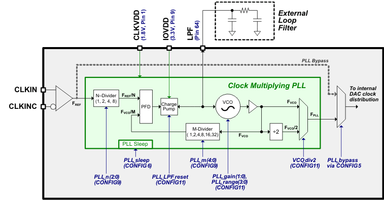 Figure 44. Functional Block Diagram for PLL
8.4.4 Recommended Multi-DAC Synchronization Procedure
The DAC5682Z provides a mechanism to synchronize multiple DAC devices in a system. The procedure has two steps involving control of the CONFIG5 clkdiv_sync_dis as well as external control of the LVDS SYNCP/N input. (All DACs involved need to be configured to accept the external SYNCP/N input and not "software" sync mode).
- Synchronize Clock Dividers (for each DAC):
- Synchronize FIFO pointers (for each DAC):
- Set CONFIG5 clkdiv_sync_dis = 1 (Disable clock divider re-sync).
- Wait a minimum of 50 CLKIN cycles from previous SYNCP/N toggle. In practice, the time required to write the above register value will typically occupy more than 50 cycles.
- Assert SYNCP/N input and hold at 1 to all DACs simultaneously. Holding this at 1 is effectively the TXENABLE for the chip so data will be output on the analog pins.
- After the normal pipeline delay of the device, the outputs of all DACs will be synchronized to within ±1 DAC clock cycle.
8.4.5 Digital Self Test Mode
The DAC5682Z has a Digital Self Test (SLFTST) mode to designed to enable board level testing without requiring specific input data test patterns. The SLFTST mode is enabled via the CONFIG1 SLFTST_ena bit and results are only valid when CONFIG3 SLFTST_err_mask bit is cleared. An internal Linear Feedback Shift Register (LFSR) is used to generate the input test patterns for the full test cycle while a checksum result is computed on the digital signal chain outputs. The LVDS input data bus is ignored in SLFTST mode. After the test cycle completes, if the checksum result does not match a hardwired comparison value, the STATUS4 SLFTST_err bit is set and will remain set until cleared by writing a ‘0’ to the SLFTST_err bit. A full self test cycle requires no more than 400,000 CLKIN/C clock cycles to complete and will automatically repeat until the SLFTEST_ena bit is cleared.
To initiate a the Digital Self Test:
- Provide a normal CLKIN/C input clock. (The PLL is not used in SLFTST mode)
- Provide a RESETB pulse to perform a hardware reset on device.
- Program the registers with the values shown in Table 6. These register values contain the settings to properly configure the SLFTST including SLFTST_ena and SLFTST_err_mask bits
- Provide a ‘1’ on the SYNCP/N input to initiate TXENABLE.
- Wait at a minimum of 400,000 CLKIN/C cycles for the SLFTST to complete. Example: If CLKIN = 1GHz, then the wait period is 400,000 × 1 / 1GHz = 400 μSec.
- Read STATUS4 SLFTST_err bit. If set, a self test error has occurred. The SLFTST_err status may optionally be programmed to output on the SDO pin if using the 3-bit SIF interface. See Table 6 Note (1).
- (Optional) The SLFTST function automatically repeats until SLFTST_ena bit is cleared. To the loop the test, write a ‘0’ to STATUS4 SLFTST_err to clear previous errors and continue at step 5 above.
- To continue normal operating mode, provide another RESETB pulse and reprogram registers to the desired normal settings.
Table 6. Digital Self Test (SLFTST) Register Values
| REGISTER | ADDRESS (hex) | VALUE (Binary) | VALUE (Hex) |
|---|---|---|---|
| CONFIG1 | 01 | 00011000 | 18 |
| CONFIG2 | 02 | 11101010 | EA |
| CONFIG3 | 03 | 10110000 | B0 |
| STATUS4 | 04 | 00000000 | 00 |
| CONFIG5 | 05 | 00000110 | 06 |
| CONFIG6 | 06 | 00001111 | 0F |
| CONFIG12 | 0C | 00001010 | 0A |
| CONFIG13 | 0D | 01010101 | 55 |
| CONFIG14(1) | 0E | 00001010 | 0A |
| CONFIG15 | 0F | 10101010 | AA |
| All others | – | Default | Default |
8.5 Programming
8.5.1 Serial Interface
The serial port of the DAC5682Z is a flexible serial interface which communicates with industry standard microprocessors and microcontrollers. The interface provides read/write access to all registers used to define the operating modes of DAC5682Z. It is compatible with most synchronous transfer formats and can be configured as a 3 or 4 pin interface by SIF4 in register CONFIG5. In both configurations, SCLK is the serial interface input clock and SDENB is serial interface enable. For 3 pin configuration, SDIO is a bidirectional pin for both data in and data out. For 4 pin configuration, SDIO is data in only and SDO is data out only. Data is input into the device with the rising edge of SCLK. Data is output from the device on the falling edge of SCLK.
Each read/write operation is framed by signal SDENB (Serial Data Enable Bar) asserted low for 2 to 5 bytes, depending on the data length to be transferred (1–4 bytes). The first frame byte is the instruction cycle which identifies the following data transfer cycle as read or write, how many bytes to transfer, and what address to transfer the data. indicates the function of each bit in the instruction cycle and is followed by a detailed description of each bit. Frame bytes 2 to 5 comprise the data transfer cycle.
| MSB | LSB | |||||||
| Bit | 7 | 6 | 5 | 4 | 3 | 2 | 1 | 0 |
| Description | R/W | N1 | N0 | A4 | A3 | A2 | A1 | A0 |
| R/W | Identifies the following data transfer cycle as a read or write operation. A high indicates a read operation from DAC5682Z and a low indicates a write operation to DAC5682Z. | ||
| [N1 : N0] | Identifies the number of data bytes to be transferred per Table 5 below. Data is transferred MSB first. | ||
Table 7. Number of Transferred Bytes Within One Communication Frame
| N1 | N0 | Description |
|---|---|---|
| 0 | 0 | Transfer 1 Byte |
| 0 | 1 | Transfer 2 Bytes |
| 1 | 0 | Transfer 3 Bytes |
| 1 | 1 | Transfer 4 Bytes |
| [A4 : A0] | Identifies the address of the register to be accessed during the read or write operation. For multi-byte transfers, this address is the starting address. Note that the address is written to the DAC5682Z MSB first and counts down for each byte. | ||
Figure 45 shows the serial interface timing diagram for a DAC5682Z write operation. SCLK is the serial interface clock input to DAC5682Z. Serial data enable SDENB is an active low input to DAC5682Z. SDIO is serial data in. Input data to DAC5682Z is clocked on the rising edges of SCLK.
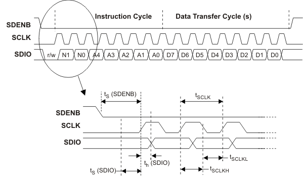 Figure 45. Serial Interface Write Timing Diagram
Figure 46 shows the serial interface timing diagram for a DAC5682Z read operation. SCLK is the serial interface clock input to DAC5682Z. Serial data enable SDENB is an active low input to DAC5682Z. SDIO is serial data in during the instruction cycle. In 3 pin configuration, SDIO is data out from DAC5682Z during the data transfer cycle(s), while SDO is in a high-impedance state. In 4 pin configuration, SDO is data out from DAC5682Z during the data transfer cycle(s). At the end of the data transfer, SDO will output low on the final falling edge of SCLK until the rising edge of SDENB when it will 3-state.
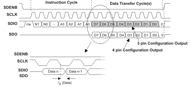 Figure 46. Serial Interface Read Timing Diagram
8.6 Register Maps
The primary modes of operation, listed in Table 8, are selected by registers CONFIG1, CONFIG2, and CONFIG3.
Table 8. DAC5682Z Modes of Operation
| Mode Name | No. of DACs Out | Interp. Factor | FIR0, CMIX0 Mode | FIR1, CMIX1 Mode | Device Config. | LVDS Input Data Mode | Max CLKIN Freq (MHz)(1) | Max DCLK Freq [DDR] (MHz) | Max Total Input Bus Rate (MSPS) | Max Input Data Rate Per Chan (#Ch @ MSPS) | Max Signal BW Per DAC (MHz) (2) |
|---|---|---|---|---|---|---|---|---|---|---|---|
| 1X1 (Bypass) | 1 | X1 | – | – | Single Real | A | 1000 | 500 | 1000 | 1 at 1000 | 500 |
| 1X2 | 1 | X2 | – | LP | Single Real | A | 1000 | 250 | 500 | 1 at 500 | 200 |
| 1X2 HP | 1 | X2 | – | HP | Single Real | A | 1000 | 250 | 500 | 1 at 500 | 200 |
| 1X4 | 1 | X4 | LP | LP | Single Real | A | 1000 | 125 | 250 | 1 at 250 | 100 |
| 1X4 LP/HP | 1 | X4 | LP | HP | Single Real | A | 1000 | 125 | 250 | 1 at 250 | 100 |
| 1X4 HP/LP | 1 | X4 | HP | LP | Single Real | A | 1000 | 125 | 250 | 1 at 250 | 50 |
| 1X4 HP/HP | 1 | X4 | HP | HP | Single Real | A | 1000 | 125 | 250 | 1 at 250 | 50 |
| 2X1 | 2 | X1 | – | – | Dual Real | A/B | 500 | 500 | 1000 | 2 at 500 | 250 |
| 2X2 | 2 | X2 | – | LP | Dual Real | A/B | 1000 | 500 | 1000 | 2 at 500 | 200 |
| 2X2 HP | 2 | X2 | – | HP | Dual Real | A/B | 1000 | 500 | 1000 | 2 at 500 | 200 |
| 2X2 CMIX | 2 | X2 | – | LP, Fs/4 | Complex | A/B | 1000 | 500 | 1000 | 2 at 500 | 200 |
| 2X4 | 2 | X4 | LP | LP | Dual Real | A/B | 1000 | 250 | 500 | 2 at 250 | 100 |
| 2X4 LP/HP | 2 | X4 | LP | HP | Dual Real | A/B | 1000 | 250 | 500 | 2 at 250 | 100 |
| 2X4 CMIX | 2 | X4 | LP | LP, Fs/4 | Complex | A/B | 1000 | 250 | 500 | 2 at 250 | 100 |
| 2X4 HP/LP | 2 | X4 | HP | LP | Dual Real | A/B | 1000 | 250 | 500 | 2 at 250 | 50 |
| 2X4 HP/HP | 2 | X4 | HP | HP | Dual Real | A/B | 1000 | 250 | 500 | 2 at 250 | 50 |
Table 9. Register Map
8.6.1 Register Name: STATUS0 – Address: 0x00, Default = 0x03
| 7 | 6 | 5 | 4 | 3 | 2 | 1 | 0 |
| PLL_lock | DLL_lock | Unused | device_ID(2:0) | version(1:0) | |||
| 0 | 0 | 0 | 0 | 0 | 0 | 1 | 1 |
| PLL_lock: | Asserted when the internal PLL is locked. (Read Only) | ||
| DLL_lock: | Asserted when the internal DLL is locked. Once the DLL is locked, this bit should remain a ‘1’ unless the DCLK input clock is removed or abruptly changes frequency causing the DLL to fall out of lock. (Read Only) | ||
| device_ID(2:0): | Returns ‘000’ for DAC5682Z Device_ID code. (ReadOnly) | ||
| version(1:0): | A hardwired register that contains the register set version of the chip. (ReadOnly) | ||
| version (1:0) | Identification | ||
| ‘01’ ‘10’ ‘11' |
PG1.0 Initial Register Set PG1.1 Register Set Production Register Set |
||
8.6.2 Register Name: CONFIG1 – Address: 0x01, Default = 0x10
| 7 | 6 | 5 | 4 | 3 | 2 | 1 | 0 |
| DAC_delay(1:0) | Unused | FIR_ena | SLFTST_ena | FIFO_offset(2:0) | |||
| 0 | 0 | 0 | 1 | 0 | 0 | 0 | 0 |
| DAC_delay(1:0): | DAC data delay adjustment. (0–3 periods of the DAC clock) This can be used to adjust system level output timing. The same delay is applied to both DACA and DACB data paths. | ||
| FIR_ena: | When set, the interpolation filters are enabled. | ||
| SLFTST_ena: | When set, a Digital Self Test (SLFTST) of the core logic is enabled. Refer to Digital Self Test Mode for details on SLFTST operation. | ||
| FIFO_offset(2:0): | Programs the output pointer location of the FIFO, allowing the input pointer to be shifted –4 to +3 positions upon SYNC. Default offset is 0 and is updated upon each sync event. | ||
| FIFO_offset(2:0) | Offset |
|---|---|
| 011 | +3 |
| 010 | +2 |
| 001 | +1 |
| 000 | 0 |
| 111 | –1 |
| 110 | –2 |
| 101 | –3 |
| 100 | –4 |
8.6.3 Register Name: CONFIG2 – Address: 0x02, Default = 0xC0
| 7 | 6 | 5 | 4 | 3 | 2 | 1 | 0 |
| Twos_comp | dual_DAC | FIR2x4x | Unused | CMIX1_mode(1:0) | CMIX0_mode(1:0) | ||
| 1 | 1 | 0 | 0 | 0 | 0 | 0 | 0 |
| Twos_comp: | When set (default) the input data format is expected to be 2’s complement, otherwise offset binary format is expected. | ||
| dual_DAC: | Selects between dual DAC mode (default) and single DAC mode. This bit is also used to select input interleaved data. | ||
| FIR2x4x: | When set, 4X interpolation of the input data is performed, otherwise 2X interpolation. | ||
| CMIX1_mode(1:0): | Determines the mode of FIR1 and final CMIX1 blocks. Settings apply to both A and B channels. Refer to Table 3 for a detailed description of CMIX1 modes. | ||
| Mode | CMIX1_mode(1) | CMIX1_mode(0) |
|---|---|---|
| Normal (Low Pass) | 0 | 0 |
| High Pass | 0 | 1 |
| +FDAC /4 | 1 | 0 |
| –FDAC/4 | 1 | 1 |
| CMIX0_mode(1:0): | Determines the mode of FIR0 and CMIX0 blocks. Because CMIX0 is located between FIR0 and FIR1, its output is half-rate. Refer to Table 2 for a detailed description of CMIX0 modes. The table below shows the effective Fs/4 or ±Fs/8 mixing with respect to the final DAC sample rate. Settings apply to both A and B channels. | ||
| Mode | CMIX1_mode(1) | CMIX1_mode(0) |
|---|---|---|
| Normal (Low Pass) | 0 | 0 |
| High Pass | 0 | 1 |
| +FDAC /8 | 1 | 0 |
| –FDAC/8 | 1 | 1 |
8.6.4 Register Name: CONFIG3 – Address: 0x03, Default = 0x70
| 7 | 6 | 5 | 4 | 3 | 2 | 1 | 0 |
| DAC_offset _ena |
SLFTST_err _mask | FIFO_err_ mask | Pattern_err_ mask | SwapAB_out | B_equals_A | SW_sync | SW_sync_sel |
| 0 | 1 | 1 | 1 | 0 | 0 | 0 | 0 |
| DAC_offset_ena: | When set, the values of OffsetA(12:0) and OffsetB(12:0) in CONFIG12 through CONFIG15 registers are summed into the DAC-A and DAC-B data paths. This provides a system-level offset adjustment capability that is independent of the input data. | ||
| SLFTST_err_mask: | When set, masks out the SLFTST_err bit in STATUS4 register. Refer to Digital Self Test Mode for details on SLFTST operation. | ||
| FIFO_err_mask: | When set, masks out the FIFO_err bit in STATUS4 register. | ||
| Pattern_err_mask: | When set, masks out the Pattern err bit in STATUS4 register. | ||
| SwapAB_out: | When set, the A/B data paths are swapped prior to routing to the DAC-A and DAC-B outputs. | ||
| B_equals_A: | When set, the data routed to DAC-A is also routed to DAC-B. This allows wire OR’ing of the two DAC outputs together at the board level to create a 2X drive strength single DAC output. | ||
| SW_sync: | This bit can be used as a substitute for the LVDS external SYNC input pins for both synchronization and transmit enable control. | ||
| SW_sync_sel: | When set, the SW_sync bit is used as the only synchronization input and the LVDS external SYNC input pins are ignored. | ||
8.6.5 Register Name: STATUS4 – Address: 0x04, Default = 0x00
| 7 | 6 | 5 | 4 | 3 | 2 | 1 | 0 |
| Unused | SLFTST_err | FIFO_err | Pattern_err | Unused | Unused | Unused | Unused |
| 0 | 0 | 0 | 0 | 0 | 0 | 0 | 0 |
| SLFTST_err: | Asserted when the Digital Self Test (SLFTST) fails. To clear the error, write a ‘0’ to this register bit. This bit is also output on the SDO pin when the Self Test is enabled via SLFTST_ena control bit in CONFIG1. Refer to Digital Self Test Mode for details on SLFTST operation. | ||
| FIFO_err: | Asserted when the FIFO pointers over run each other causing a sample to be missed. To clear the error, write a ‘0’ to this register bit. | ||
| Pattern_err: | A digital checkerboard pattern compare function is provided for board level confidence testing and DLL limit checks. If the Pattern_err_mask bit via CONFIG3 is cleared, logic is enabled to continuously monitor input FIFO data. Any received data pattern other than 0xAAAA or 0x5555 causes this bit to be set. To clear the error, flush out the previous pattern error by inputting at least 8 samples of the 0xAAAA and/or 0x5555, then write a ‘0’ to this register bit. | ||
8.6.6 Register Name: CONFIG5 – Address: 0x05, Default = 0x00
| 7 | 6 | 5 | 4 | 3 | 2 | 1 | 0 |
| SIF4 | rev_bus | clkdiv_sync _dis | Reserved | Reserved | DLL_bypass | PLL_bypass | Reserved |
| 0 | 0 | 0 | 0 | 0 | 0 | 0 | 0 |
8.6.7 Register Name: CONFIG6 – Address: 0x06, Default = 0x0C
| 7 | 6 | 5 | 4 | 3 | 2 | 1 | 0 |
| Reserved | Unused | Sleep_B | Sleep_A | BiasLPF_A | BiasLPF_B | PLL_sleep | DLL_sleep |
| 0 | 0 | 0 | 0 | 1 | 1 | 0 | 0 |
8.6.8 Register Name: CONFIG7 – Address: 0x07, Default = 0xFF
| 7 | 6 | 5 | 4 | 3 | 2 | 1 | 0 |
| DACA_gain(3:0) | DACB_gain(3:0) | ||||||
| 1 | 1 | 1 | 1 | 1 | 1 | 1 | 1 |
| DACA_gain(3:0): | Scales DACA output current in 16 equal steps. | ||
 |
|||
| DACB_gain(3:0): | Same as above except for DACB. | ||
8.6.9 Register Name: CONFIG8 – Address: 0x08, Default = 0x00
| 7 | 6 | 5 | 4 | 3 | 2 | 1 | 0 |
| Reserved | DLL_restart | Reserved | |||||
| 0 | 0 | 0 | 0 | 0 | 0 | 0 | 0 |
| Reserved (7:3): | Set to ‘00000’ for proper operation. | ||
| DLL_restart: | This bit is used to restart the DLL. When this bit is set, the internal DLL loop filter is reset to zero volts, and the DLL delay line is held at the center of its bias range. When cleared, the DLL will acquire lock to the DCLK signal. A DLL restart is accomplished by setting this bit with a serial interface write, and then clearing this bit with another serial interface write. Any interruption in the DCLK signal or changes to the DLL programming in the CONFIG10 register must be followed by this DLL restart sequence. Also, when this bit is set, the DLL_lock indicator in the STATUS0 register is cleared. | ||
| Reserved (1:0): | Set to ‘00’ for proper operation | ||
8.6.10 Register Name: CONFIG9 – Address: 0x09, Default = 0x00
| 7 | 6 | 5 | 4 | 3 | 2 | 1 | 0 |
| PLL_m(4:0) | PLL_n(2:0) | ||||||
| 0 | 0 | 0 | 0 | 0 | 0 | 0 | 0 |
| PLL_m: | M portion of the M/N divider of the PLL thermometer encoded: | ||
| PLL_m(4:0) | M value |
|---|---|
| 00000 | 1 |
| 00001 | 2 |
| 00011 | 4 |
| 00111 | 8 |
| 01111 | 16 |
| 11111 | 32 |
| All other values | Invalid |
| PLL_n: | N portion of the M/N divider of the PLL thermometer encoded. If supplying a high rate CLKIN frequency, the PLL_n value should be used to divide down the input CLKIN to maintain a maximum PFD operating of 160 MHz. | ||
| PLL_n(2:0) | N value |
|---|---|
| 000 | 1 |
| 001 | 2 |
| 011 | 4 |
| 111 | 8 |
| All other values | Invalid |
| PLL Function: | |||
 |
|||
| where ƒref is the frequency of the external DAC clock input on the CLKIN/CLKINC pins. | |||
8.6.11 Register Name: CONFIG10 – Address: 0x0A, Default = 0x00
| 7 | 6 | 5 | 4 | 3 | 2 | 1 | 0 |
| DLL_delay(3:0) | DLL_invclk | DLL_ifixed(2:0) | |||||
| 0 | 0 | 0 | 0 | 0 | 0 | 0 | 0 |
| DLL_delay(3:0): | The DCLKP/N LVDS input data clock has a DLL to automatically skew the clock to LVDS data timing relationship, providing proper setup and hold times. DLL_delay(3:0) is used to manually adjust the DLL delay ± from the fixed delay set by DLL_ifixed(2:0). Adjustment amounts are approximate. | ||
| DLL_delay(3:0) | Delay Adjust (degrees) |
|---|---|
| 1000 | 50° |
| 1001 | 55° |
| 1010 | 60° |
| 1011 | 65° |
| 1100 | 70° |
| 1101 | 75° |
| 1110 | 80° |
| 1111 | 85° |
| 0000 | 90° (Default) |
| 0001 | 95° |
| 0010 | 100° |
| 0011 | 105° |
| 0100 | 110° |
| 0101 | 115° |
| 0110 | 120° |
| 0111 | 125° |
| DLL_invclk: | When set, used to invert an internal DLL clock to force convergence to a different solution. This can be used in the case where the DLL delay adjustment has exceeded the limits of its range. | ||
| DLL_ifixed(2:0): | Adjusts the DLL delay line bias current. Refer to the Electrical Characteristics table. Used in conjunction with the DLL_invclk bit to select appropriate delay range for a given DCLK frequency: '011' – maximum bias current and minimum delay range '000' – mid scale bias current '101' – minimum bias current and maximum delay range '100' – do not use. |
||
8.6.12 Register Name: CONFIG11 – Address: 0x0B, Default = 0x00
| 7 | 6 | 5 | 4 | 3 | 2 | 1 | 0 |
| PLL_LPF_ reset | VCO_div2 | PLL_gain(1:0) | PLL_range(3:0) | ||||
| 0 | 0 | 0 | 0 | 0 | 0 | 0 | 0 |
| PLL_LPF_reset: | When a logic high, the PLL loop filter (LPF) is pulled down to 0V. Toggle from ‘1’ to ‘0’ to restart the PLL if an over-speed lock-up occurs. Over-speed can happen when the process is fast, the supplies are higher than nominal, etc., resulting in the feedback dividers missing a clock. | ||
| VCO_div2: | When set, the PLL CLOCK output is 1/2 the PLL VCO frequency. Used to run the VCO at 2X the needed clock frequency to reduce phase noise for lower input clock rates. | ||
| PLL_gain(1:0): | Used to adjust the PLL Voltage Controlled Oscillator (VCO) gain, KVCO. Refer to the Electrical Characteristics table. By increasing the PLL_gain, the VCO can cover a broader range of frequencies; however, the higher gain also increases the phase noise of the PLL. In general, lower PLL_gain settings result in lower phase noise. The KVCO of the VCO can also affect the PLL stability and is used to determine the loop filter components. See section on determining the PLL filter components for more detail. | ||
| PLL_range(3:0): | Programs the PLL VCO fixed bias current. Refer to the Electrical Characteristics table. This setting, in conjunction with the PLL_gain(1:0), sets the achievable frequency range of the PLL VCO: '000' – minimum bias current and lowest VCO frequency range '111' – maximum bias current and highest VCO frequency range |
||
8.6.13 Register Name: CONFIG12 – Address: 0x0C, Default = 0x00
| 7 | 6 | 5 | 4 | 3 | 2 | 1 | 0 |
| Reserved(1:0) | Offset_sync | OffsetA(12:8) | |||||
| 0 | 0 | 0 | 0 | 0 | 0 | 0 | 0 |
| Reserved(1:0): | Set to ‘00’ for proper operation. | ||
| Offset_sync: | On a change from ‘0’ to ‘1’ the values of the OffsetA(12:0) and OffsetB(12:0) control registers are transferred to the registers used in the DAC-A and DAC-B offset calculations. This double buffering allows complete control by the user as to when the change in the offset value occurs. This bit does not auto-clear. Prior to updating new offset values, it is recommended that the user clear this bit. | ||
| OffsetA(12:8): | Upper 5 bits of the offset adjustment value for the A data path. (SYNCED via Offset_sync) | ||
8.6.14 Register Name: CONFIG13 – Address: 0x0D, Default = 0x00
| 7 | 6 | 5 | 4 | 3 | 2 | 1 | 0 |
| OffsetA(7:0) | |||||||
| 0 | 0 | 0 | 0 | 0 | 0 | 0 | 0 |
| OffsetA(7:0): | Lower 8 bits of the offset adjustment value for the A data path. (SYNCED via Offset_sync) | ||
8.6.15 Register Name: CONFIG14 – Address: 0x0E, Default = 0x00
| 7 | 6 | 5 | 4 | 3 | 2 | 1 | 0 |
| SDO_func_sel(2:0) | OffsetB(12:8) | ||||||
| 0 | 0 | 0 | 0 | 0 | 0 | 0 | 0 |
| SDO_func_sel(2:0): | Selects the signal for output on the SDO pin. When using the 3 pin serial interface mode, this allows the user to multiplex several status indicators onto the SDO pin. In 4 pin serial interface mode, programming this register to view one of the 5 available status indicators will override normal SDO serial interface operation. | ||
| SDO_func_sel (2:0) |
Output to SDO |
|---|---|
| 000, 110, 111 | Normal SDO function |
| 001 | PLL_lock |
| 010 | DLL_lock |
| 011 | Pattern_err |
| 100 | FIFO_err |
| 101 | SLFTST_err |
| OffsetB(12:8): | Upper 5 bits of the offset adjustment value for the B data path. (SYNCED via Offset_sync) | ||
8.6.16 Register Name: CONFIG15 – Address: 0x0F, Default = 0x00
| 7 | 6 | 5 | 4 | 3 | 2 | 1 | 0 |
| OffsetB(7:0) | |||||||
| 0 | 0 | 0 | 0 | 0 | 0 | 0 | 0 |
| OffsetB(7:0): | Lower 8 bits of the offset adjustment value for the B data path. (SYNCED via Offset_sync) | ||