ZHCSI68F September 2007 – October 2018 DAC5652A
PRODUCTION DATA.
- 1 特性
- 2 应用
- 3 说明
- 4 修订历史记录
- 5 Pin Configuration and Functions
-
6 Specifications
- 6.1 Absolute Maximum Ratings
- 6.2 ESD Ratings
- 6.3 Recommended Operating Conditions
- 6.4 Thermal Information
- 6.5 Electrical Characteristics: DC
- 6.6 Electrical Characteristics: AC
- 6.7 Electrical Characteristics: Digital Input
- 6.8 Electrical Characteristics: Power Supply
- 6.9 Switching Characteristics
- 6.10 Typical Characteristics
- 7 Detailed Description
- 8 Application and Implementation
- 9 Power Supply Recommendations
- 10Layout
- 11器件和文档支持
- 12机械、封装和可订购信息
封装选项
机械数据 (封装 | 引脚)
散热焊盘机械数据 (封装 | 引脚)
- RSL|48
订购信息
7.3.1 Digital Inputs
The data input ports of the DAC5652A accept a standard positive coding with data bits DA9 and DB9 being the most significant bits (MSB). The converter outputs support a clock rate of up to 275 MSPS. The best performance is typically achieved with a symmetric duty cycle for write and clock; however, the duty cycle may vary as long as the timing specifications are met. Similarly, the setup and hold times may be chosen within their specified limits.
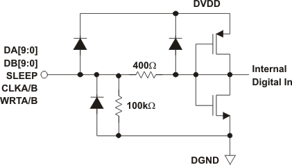
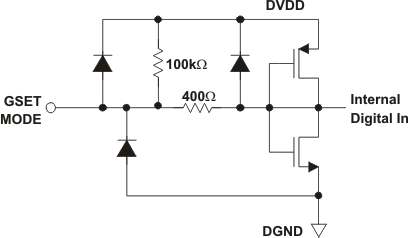
All digital inputs of the DAC5652A are CMOS compatible. Figure 13 and Figure 14 show schematics of the equivalent CMOS digital inputs of the DAC5652A. The pullup and pulldown circuitry is approximately equivalent to 100 kΩ. The 10-bit digital data input follows the offset positive binary coding scheme. The DAC5652A is designed to operate with a digital supply (DVDD) of 3 V to 3.6 V.

