ZHCSG79C April 2017 – April 2018 CSD88599Q5DC
PRODUCTION DATA.
- 1特性
- 2应用
- 3说明
- 4修订历史记录
- 5Specifications
-
6Application and Implementation
- 6.1 Application Information
- 6.2 Brushless DC Motor With Trapezoidal Control
- 6.3 Power Loss Curves
- 6.4 Safe Operating Area (SOA) Curve
- 6.5 Normalized Power Loss Curves
- 6.6 Design Example – Regulate Current to Maintain Safe Operation
- 6.7 Design Example – Regulate Board and Case Temperature to Maintain Safe Operation
- 7Layout
- 8器件和文档支持
- 9机械、封装和可订购信息
7.2 Layout Example
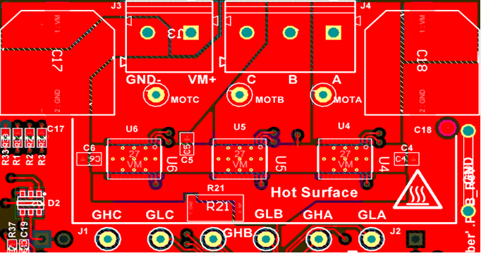
 Figure 23. Top Layer Figure 23. Top Layer |
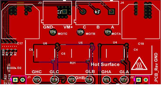
 Figure 24. Bottom Layer Figure 24. Bottom Layer |
The placement of the input capacitors C4, C5, and C6 relative to VIN and PGND pins of CSD88599Q5DC device should have the highest priority during the component placement routine. It is critical to minimize the VIN to GND parasitic loop inductance. A shunt resistor R21 is used between all three U4, U5, and U6 power block source terminals to the input supply GND return pin.
Input RMS current filtering is achieved via two bulk caps C17 and C18. Based on the RMS current ratings, the recommended part number for input bulk is CAP AL, 330 µF, 63 V, ±20%, PN: EMVA630ADA331MKG5S.