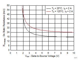
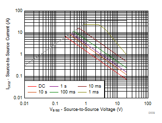
| STATIC CHARACTERISTICS |
| BVS1S2 |
Source-to-source voltage |
VGS = 0 V, IS = 250 μA |
20 |
|
|
V |
| IS1S2 |
Source-to-source leakage current |
VGS = 0 V, VS1S2 = 16 V |
|
|
1 |
μA |
| IGSS |
Gate-to-source leakage current |
VS1S2 = 0 V, VGS = 6 V |
|
|
0.5 |
µA |
| VS1S2 = 0 V, VGS = 10V |
|
|
4 |
µA |
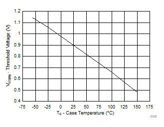
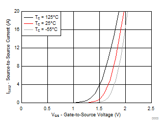
| VGS(th) |
Gate-to-source threshold voltage |
VS1S2 = VGS, IS = 250 μA |
0.68 |
0.9 |
1.3 |
V |
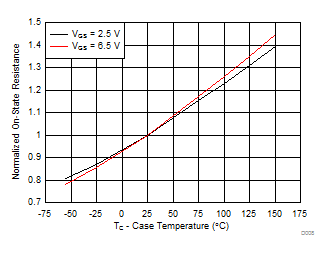
| RS1S2(on) |
Source-to-source on-resistance |
VGS = 2.5 V, IS = 2 A |
20 |
29 |
36 |
mΩ |
| VGS = 4.5 V, IS = 2 A |
14 |
20 |
24 |
mΩ |
| VGS = 6.5 V, IS = 2 A |
13 |
18.7 |
22.5 |
mΩ |
| gfs |
Transconductance |
VS1S2 = 2 V, IS = 2 A |
|
19 |
|
S |
| DYNAMIC CHARACTERISTICS(1) |
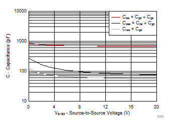
| Ciss |
Input capacitance |
VGS = 0 V, VS1S2 = 10 V, ƒ = 1 MHz |
|
718 |
933 |
pF |
| Coss |
Output capacitance |
|
92 |
120 |
pF |
| Crss |
Reverse transfer capacitance |
|
61 |
79 |
pF |
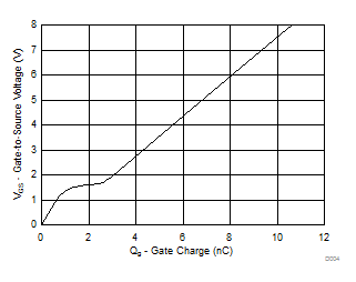
| Qg |
Gate charge total (4.5 V) |
VS1S2 = 10 V, IS = 2 A |
|
6.0 |
7.8 |
nC |
| Qgd |
Gate charge gate-to-drain |
|
1.4 |
|
nC |
| Qgs |
Gate charge gate-to-source |
|
1.2 |
|
nC |
| Qg(th) |
Gate charge at Vth |
|
0.6 |
|
nC |
| Qoss |
Output charge |
VS1S2 = 10 V, VGS = 0 V |
|
2.3 |
|
nC |
| td(on) |
Turn-on delay time |
VS1S2 = 10 V, VGS = 4.5 V,
IS1S2 = 2 A, RG = 0 Ω |
|
37 |
|
ns |
| tr |
Rise time |
|
54 |
|
ns |
| td(off) |
Turn-off delay time |
|
173 |
|
ns |
| tf |
Fall time |
|
99 |
|
ns |
