SCAS871H February 2009 – January 2016 CDCM61004
PRODUCTION DATA.
- 1 Features
- 2 Applications
- 3 Description
- 4 Revision History
- 5 Description (Continued)
- 6 Pin Configuration and Functions
-
7 Specifications
- 7.1 Absolute Maximum Ratings
- 7.2 ESD Ratings
- 7.3 Recommended Operating Conditions
- 7.4 Thermal Information
- 7.5 Electrical Characteristics
- 7.6 Typical Output Phase Noise CharacteristicsCorrected units for tRJIT (RMS phase jitter); changed to fs, RMS from ps, RMS
- 7.7 Typical Output Jitter Characteristics
- 7.8 Crystal Characteristics
- 7.9 Dissipation Ratings
- 7.10 Typical Characteristics
- 8 Parameter Measurement Information
-
9 Detailed Description
- 9.1 Overview
- 9.2 Functional Block Diagram
- 9.3
Feature Description
- 9.3.1 Phase-Locked Loop (PLL)
- 9.3.2 Configuring the PLL
- 9.3.3 Crystal Input Interface
- 9.3.4 Phase Frequency Detector (PFD)
- 9.3.5 Charge Pump (CP)
- 9.3.6 On-Chip PLL Loop Filter
- 9.3.7 Prescaler Divider and Feedback Divider
- 9.3.8 On-Chip VCO
- 9.3.9 LVCMOS Input Interface
- 9.3.10 Output Divider
- 9.3.11 Output Buffer
- 9.4 Device Functional Modes
- 10Application and Implementation
- 11Power Supply Recommendations
- 12Layout
- 13Device and Documentation Support
- 14Mechanical, Packaging, and Orderable Information
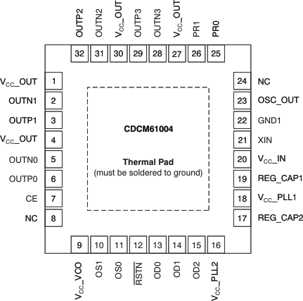
6 Pin Configuration and Functions
RHB Package
32-Pin VQFN
Top View

Pin Functions
| PIN | TYPE | DIRECTION(1) | DESCRIPTION | |
|---|---|---|---|---|
| NAME | NO. | |||
| CE | 7 | Input | Pullup | Chip enable control pin (see Table 7) |
| GND1 | 22 | Ground | — | Additional ground for device. (GND1 shorted on-chip to GND) |
| GND | Pad | Ground | — | Ground is on thermal pad. See Thermal Management |
| NC | 8, 24 | — | — | No connection |
| OD2, OD1, OD0 | 15, 14, 13 | Input | Pullup | Output divider control pins (see Table 5) |
| OS1, OS0 | 10, 11 | Input | Pullup | Output type select control pin (see Table 6) |
| OSC_OUT | 23 | Output | — | Bypass LVCMOS output |
| OUTP0, OUTN0 | 6, 5 | Output | — | Differential output pair or two single-ended outputs |
| OUTP1, OUTN1 | 3, 2 | Output | — | Differential output pair or two single-ended outputs |
| OUTP2, OUTN2 | 32, 31 | Output | — | Differential output pair or two single-ended outputs |
| OUTP3, OUTN3 | 29, 28 | Output | — | Differential output pair or two single-ended outputs |
| PR1, PR0 | 26, 25 | Input | Pullup | Prescaler and Feedback divider control pins (see Table 4) |
| REG_CAP1 | 19 | Output | — | Capacitor for internal regulator (connect to a 10-μF Y5V capacitor to GND) |
| REG_CAP2 | 17 | Output | — | Capacitor for internal regulator (connect to a 10-μF Y5V capacitor to GND) |
| RSTN | 12 | Input | Pullup | Device reset (active low) (see Table 8) |
| VCC_OUT | 1, 4, 27, 30 | Power | — | 3.3-V supply for the output buffers |
| VCC_PLL1 | 18 | Power | — | 3.3-V supply for the PLL circuitry |
| VCC_PLL2 | 16 | Power | — | 3.3-V supply for the PLL circuitry |
| VCC_VCO | 9 | Power | — | 3.3-V supply for the internal VCO |
| VCC_IN | 20 | Power | — | 3.3-V supply for the input buffers |
| XIN | 21 | Input | — | Parallel resonant crystal or LVCMOS inputs |
(1) Pullup refers to internal input resistors; see Pin Characteristics, Pin Characteristics for typical values.