SCAS871H February 2009 – January 2016 CDCM61004
PRODUCTION DATA.
- 1 Features
- 2 Applications
- 3 Description
- 4 Revision History
- 5 Description (Continued)
- 6 Pin Configuration and Functions
-
7 Specifications
- 7.1 Absolute Maximum Ratings
- 7.2 ESD Ratings
- 7.3 Recommended Operating Conditions
- 7.4 Thermal Information
- 7.5 Electrical Characteristics
- 7.6 Typical Output Phase Noise CharacteristicsCorrected units for tRJIT (RMS phase jitter); changed to fs, RMS from ps, RMS
- 7.7 Typical Output Jitter Characteristics
- 7.8 Crystal Characteristics
- 7.9 Dissipation Ratings
- 7.10 Typical Characteristics
- 8 Parameter Measurement Information
-
9 Detailed Description
- 9.1 Overview
- 9.2 Functional Block Diagram
- 9.3
Feature Description
- 9.3.1 Phase-Locked Loop (PLL)
- 9.3.2 Configuring the PLL
- 9.3.3 Crystal Input Interface
- 9.3.4 Phase Frequency Detector (PFD)
- 9.3.5 Charge Pump (CP)
- 9.3.6 On-Chip PLL Loop Filter
- 9.3.7 Prescaler Divider and Feedback Divider
- 9.3.8 On-Chip VCO
- 9.3.9 LVCMOS Input Interface
- 9.3.10 Output Divider
- 9.3.11 Output Buffer
- 9.4 Device Functional Modes
- 10Application and Implementation
- 11Power Supply Recommendations
- 12Layout
- 13Device and Documentation Support
- 14Mechanical, Packaging, and Orderable Information
8 Parameter Measurement Information
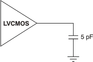
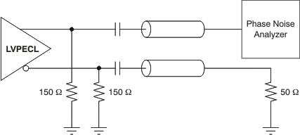
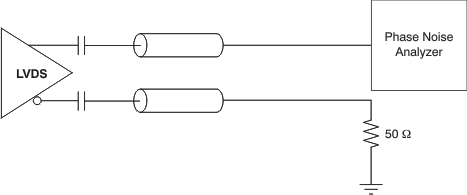
This section describes the function of each block for the CDCM61004. Figure 7 through Figure 13 illustrate how the device should be set up for a variety of output configurations.
 Figure 7. LVCMOS Output Loading During Device Test
 Figure 8. LVCMOS AC Configuration During Device Test
 Figure 9. LVPECL DC Configuration During Device Test
 Figure 10. LVPECL AC Configuration During Device Test
 Figure 11. LVDS DC Configuration During Device Test
 Figure 12. LVDS AC Configuration During Device Test
 Figure 13. Output Voltage and Rise and Fall Times