ZHCSKT0J November 1998 – August 2024 CD4066B
PRODUCTION DATA
- 1
- 1 特性
- 2 应用
- 3 说明
- 4 Pin Configuration and Functions
- 5 Specifications
- 6 Parameter Measurement Information
- 7 Detailed Description
- 8 Application and Implementation
- 9 Device and Documentation Support
- 10Revision History
- 11Mechanical, Packaging, and Orderable Information
封装选项
请参考 PDF 数据表获取器件具体的封装图。
机械数据 (封装 | 引脚)
- D|14
- PW|14
- N|14
- NS|14
散热焊盘机械数据 (封装 | 引脚)
订购信息
6 Parameter Measurement Information
 Figure 6-1 Determination of ron as a Test Condition for Control-Input
High-Voltage (VIHC) Specification
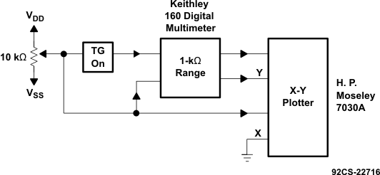
 Figure 6-2 Channel On-State Resistance Measurement Circuit
 Figure 6-3 Typical On Characteristics for One of Four Channels
 Figure 6-4 Off-Switch Input or Output Leakage
 Figure 6-5 Propagation Delay Time Signal Input (Vis) to Signal Output
(Vos)
 Figure 6-6 Crosstalk-Control Input to Signal Output
All unused
pins are connected to VSS.
Delay is
measured at Vos level of +10% from ground (turn-on) or on-state
output level (turn-off).
Figure 6-7 Propagation Delay, tPLH, tPHL Control-Signal
Output
All unused
pins are connected to VSS.
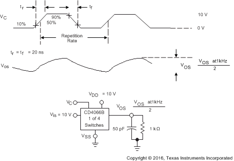
Figure 6-8 Maximum Allowable Control-Input Repetition Rate Figure 6-9 Input
Leakage-Current Test Circuit
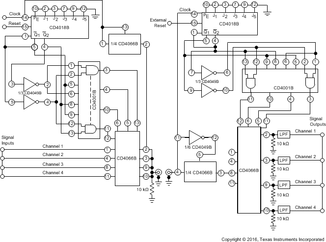
 Figure 6-10 Four-Channel PAM Multiplex System Diagram