ZHCSDE0A February 2015 – October 2015 CC2650
PRODUCTION DATA.
- 1器件概述
- 2修订历史记录
- 3 Device Comparison
- 4Terminal Configuration and Functions
-
5Specifications
- 5.1 Absolute Maximum Ratings
- 5.2 ESD Ratings
- 5.3 Recommended Operating Conditions
- 5.4 Power Consumption Summary
- 5.5 General Characteristics
- 5.6 1-Mbps GFSK (Bluetooth Low Energy) - RX
- 5.7 1-Mbps GFSK (Bluetooth Low Energy) - TX
- 5.8 IEEE 802.15.4 (Offset Q-PSK DSSS, 250 kbps) - RX
- 5.9 IEEE 802.15.4 (Offset Q-PSK DSSS, 250 kbps) - TX
- 5.10 24-MHz Crystal Oscillator (XOSC_HF)
- 5.11 32.768-kHz Crystal Oscillator (XOSC_LF)
- 5.12 48-MHz RC Oscillator (RCOSC_HF)
- 5.13 32-kHz RC Oscillator (RCOSC_LF)
- 5.14 ADC Characteristics
- 5.15 Temperature Sensor
- 5.16 Battery Monitor
- 5.17 Continuous Time Comparator
- 5.18 Low-Power Clocked Comparator
- 5.19 Programmable Current Source
- 5.20 DC Characteristics
- 5.21 Thermal Characteristics
- 5.22 Timing Requirements
- 5.23 Switching Characteristics
- 5.24 Typical Characteristics
- 6Detailed Description
- 7Application, Implementation, and Layout
- 8器件和文档支持
- 9机械、封装和可订购信息
封装选项
请参考 PDF 数据表获取器件具体的封装图。
机械数据 (封装 | 引脚)
- RSM|32
- RHB|32
- RGZ|48
散热焊盘机械数据 (封装 | 引脚)
订购信息
5 Specifications
5.1 Absolute Maximum Ratings
over operating free-air temperature range (unless otherwise noted)(1)(2)| MIN | MAX | UNIT | ||
|---|---|---|---|---|
| Supply voltage, VDDS(3) | VDDR supplied by internal DC-DC regulator or internal GLDO | –0.3 | 4.1 | V |
| Supply voltage, VDDS(3) and VDDR | External regulator mode (VDDS and VDDR pins connected on PCB) | –0.3 | 2.25 | V |
| Voltage on any digital pin(4) | –0.3 | VDDS + 0.3, max 4.1 | V | |
| Voltage on crystal oscillator pins, X32K_Q1, X32K_Q2, X24M_N and X24M_P | –0.3 | VDDR + 0.3, max 2.25 | V | |
| Voltage on ADC input (Vin) | Voltage scaling enabled | –0.3 | VDDS | V |
| Voltage scaling disabled, internal reference | –0.3 | 1.49 | ||
| Voltage scaling disabled, VDDS as reference | –0.3 | VDDS / 2.9 | ||
| Input RF level | 5 | dBm | ||
| Tstg | Storage temperature | –40 | 150 | °C |
(1) All voltage values are with respect to ground, unless otherwise noted.
(2) Stresses beyond those listed under Absolute Maximum Ratings may cause permanent damage to the device. These are stress ratings only, and functional operation of the device at these or any other conditions beyond those indicated under Recommended Operating Conditions is not implied. Exposure to absolute-maximum-rated conditions for extended periods may affect device reliability.
(3) VDDS2 and VDDS3 must be at the same potential as VDDS.
(4) Including analog-capable DIO.
5.2 ESD Ratings
| VALUE | UNIT | ||||
|---|---|---|---|---|---|
| VESD | Electrostatic discharge (ESD) performance | Human body model (HBM), per ANSI/ESDA/JEDEC JS001(1) | All pins | ±2500 | V |
| Charged device model (CDM), per JESD22-C101(2) | RF pins | ±750 | |||
| Non-RF pins | ±750 | ||||
(1) JEDEC document JEP155 states that 500-V HBM allows safe manufacturing with a standard ESD control process.
(2) JEDEC document JEP157 states that 250-V CDM allows safe manufacturing with a standard ESD control process.
5.3 Recommended Operating Conditions
over operating free-air temperature range (unless otherwise noted)| MIN | MAX | UNIT | ||
|---|---|---|---|---|
| Ambient temperature range | –40 | 85 | °C | |
| Operating supply voltage (VDDS and VDDR), external regulator mode | For operation in 1.8-V systems (VDDS and VDDR pins connected on PCB, internal DC-DC cannot be used) |
1.7 | 1.95 | V |
| Operating supply voltage (VDDS) | For operation in battery-powered and 3.3-V systems (internal DC-DC can be used to minimize power consumption) |
1.8 | 3.8 | V |
5.4 Power Consumption Summary
Measured on the TI CC2650EM-5XD reference design with Tc = 25°C, VDDS = 3.0 V with internal DC-DC converter, unless otherwise noted.| PARAMETER | TEST CONDITIONS | MIN | TYP | MAX | UNIT | |
|---|---|---|---|---|---|---|
| Icore | Core current consumption | Reset. RESET_N pin asserted or VDDS below Power-on-Reset threshold | 100 | nA | ||
| Shutdown. No clocks running, no retention | 150 | |||||
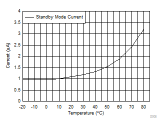
| Standby. With RTC, CPU, RAM and (partial) register retention. RCOSC_LF | 1 | µA | ||||
| Standby. With RTC, CPU, RAM and (partial) register retention. XOSC_LF | 1.2 | |||||
| Standby. With Cache, RTC, CPU, RAM and (partial) register retention. RCOSC_LF | 2.5 | |||||
| Standby. With Cache, RTC, CPU, RAM and (partial) register retention. XOSC_LF | 2.7 | |||||
| Idle. Supply Systems and RAM powered. | 550 | |||||
| Active. Core running CoreMark | 1.45 mA + 31 µA/MHz |
|||||
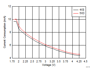
| Radio RX (1) | 5.9 | mA | ||||
| Radio RX(2) | 6.1 | |||||
| Radio TX, 0-dBm output power(1) | 6.1 | |||||
| Radio TX, 5-dBm output power(2) | 9.1 | |||||
| Peripheral Current Consumption (Adds to core current Icore for each peripheral unit activated)(3) | ||||||
| Iperi | Peripheral power domain | Delta current with domain enabled | 20 | µA | ||
| Serial power domain | Delta current with domain enabled | 13 | µA | |||
| RF Core | Delta current with power domain enabled, clock enabled, RF core idle | 237 | µA | |||
| µDMA | Delta current with clock enabled, module idle | 130 | µA | |||
| Timers | Delta current with clock enabled, module idle | 113 | µA | |||
| I2C | Delta current with clock enabled, module idle | 12 | µA | |||
| I2S | Delta current with clock enabled, module idle | 36 | µA | |||
| SSI | Delta current with clock enabled, module idle | 93 | µA | |||
| UART | Delta current with clock enabled, module idle | 164 | µA | |||
(1) Single-ended RF mode is optimized for size and power consumption. Measured on CC2650EM-4XS.
(2) Differential RF mode is optimized for RF performance. Measured on CC2650EM-5XD.
(3) Iperi is not supported in Standby or Shutdown.
5.5 General Characteristics
Measured on the TI CC2650EM-5XD reference design with Tc = 25°C, VDDS = 3.0 V, unless otherwise noted.| PARAMETER | TEST CONDITIONS | MIN | TYP | MAX | UNIT |
|---|---|---|---|---|---|
| FLASH MEMORY | |||||
| Supported flash erase cycles before failure | 100 | k Cycles | |||
| Flash page/sector erase current | Average delta current | 12.6 | mA | ||
| Flash page/sector size | 4 | KB | |||
| Flash write current | Average delta current, 4 bytes at a time | 8.15 | mA | ||
| Flash page/sector erase time(1) | 8 | ms | |||
| Flash write time(1) | 4 bytes at a time | 8 | µs | ||
(1) This number is dependent on Flash aging and will increase over time and erase cycles.
5.6 1-Mbps GFSK (Bluetooth Low Energy) – RX
Measured on the TI CC2650EM-5XD reference design with Tc = 25°C, VDDS = 3.0 V, fRF = 2440 MHz, unless otherwise noted.| PARAMETER | TEST CONDITIONS | MIN | TYP | MAX | UNIT |
|---|---|---|---|---|---|
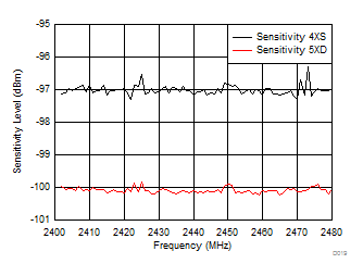
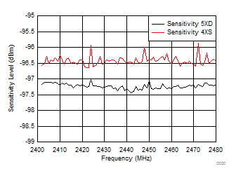
| Receiver sensitivity | Differential mode. Measured at the CC2650EM-5XD SMA connector, BER = 10–3 | –97 | dBm | ||
| Receiver sensitivity | Single-ended mode. Measured on CC2650EM-4XS, at the SMA connector, BER = 10–3 | –96 | dBm | ||
| Receiver saturation | Differential mode. Measured at the CC2650EM-5XD SMA connector, BER = 10–3 | 4 | dBm | ||
| Receiver saturation | Single-ended mode. Measured on CC2650EM-4XS, at the SMA connector, BER = 10–3 | 0 | dBm | ||
| Frequency error tolerance | Difference between the incoming carrier frequency and the internally generated carrier frequency | –350 | 350 | kHz | |
| Data rate error tolerance | Difference between incoming data rate and the internally generated data rate | –750 | 750 | ppm | |
| Co-channel rejection (2) | Wanted signal at –67 dBm, modulated interferer in channel, BER = 10–3 |
–6 | dB | ||
| Selectivity, ±1 MHz (2) | Wanted signal at –67 dBm, modulated interferer at ±1 MHz, BER = 10–3 |
7 / 3(1) | dB | ||
| Selectivity, ±2 MHz (2) | Wanted signal at –67 dBm, modulated interferer at ±2 MHz, BER = 10–3 |
34 / 25(1) | dB | ||
| Selectivity, ±3 MHz (2) | Wanted signal at –67 dBm, modulated interferer at ±3 MHz, BER = 10–3 |
38 / 26(1) | dB | ||
| Selectivity, ±4 MHz (2) | Wanted signal at –67 dBm, modulated interferer at ±4 MHz, BER = 10–3 |
42 / 29(1) | dB | ||
| Selectivity, ±5 MHz or more(2) | Wanted signal at –67 dBm, modulated interferer at ≥ ±5 MHz, BER = 10–3 | 32 | dB | ||
| Selectivity, Image frequency(2) | Wanted signal at –67 dBm, modulated interferer at image frequency, BER = 10–3 |
25 | dB | ||
| Selectivity, Image frequency ±1 MHz(2) |
Wanted signal at –67 dBm, modulated interferer at ±1 MHz from image frequency, BER = 10–3 | 3 / 26(1) | dB | ||
| Out-of-band blocking (3) | 30 MHz to 2000 MHz | –20 | dBm | ||
| Out-of-band blocking | 2003 MHz to 2399 MHz | –5 | dBm | ||
| Out-of-band blocking | 2484 MHz to 2997 MHz | –8 | dBm | ||
| Out-of-band blocking | 3000 MHz to 12.75 GHz | –8 | dBm | ||
| Intermodulation | Wanted signal at 2402 MHz, –64 dBm. Two interferers at 2405 and 2408 MHz respectively, at the given power level | –34 | dBm | ||
| Spurious emissions, 30 to 1000 MHz |
Conducted measurement in a 50-Ω single-ended load. Suitable for systems targeting compliance with EN 300 328, EN 300 440 class 2, FCC CFR47, Part 15 and ARIB STD-T-66 | –71 | dBm | ||
| Spurious emissions, 1 to 12.75 GHz |
Conducted measurement in a 50 Ω single-ended load. Suitable for systems targeting compliance with EN 300 328, EN 300 440 class 2, FCC CFR47, Part 15 and ARIB STD-T-66 | –62 | dBm | ||
| RSSI dynamic range | 70 | dB | |||
| RSSI accuracy | ±4 | dB |
(1) X / Y, where X is +N MHz and Y is –N MHz.
(2) Numbers given as I/C dB.
(3) Excluding one exception at Fwanted / 2, per Bluetooth Specification.
5.7 1-Mbps GFSK (Bluetooth Low Energy) – TX
Measured on the TI CC2650EM-5XD reference design with Tc = 25°C, VDDS = 3.0 V, fRF = 2440 MHz, unless otherwise noted.| PARAMETER | TEST CONDITIONS | MIN | TYP | MAX | UNIT |
|---|---|---|---|---|---|
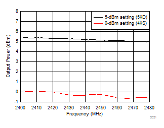
| Output power, highest setting | Differential mode, delivered to a single-ended 50-Ω load through a balun | 5 | dBm | ||
| Output power, highest setting | Measured on CC2650EM-4XS, delivered to a single-ended 50-Ω load | 2 | dBm | ||
| Output power, lowest setting | Delivered to a single-ended 50-Ω load through a balun | –21 | dBm | ||
| Spurious emission conducted measurement(1) | f < 1 GHz, outside restricted bands | –43 | dBm | ||
| f < 1 GHz, restricted bands ETSI | –65 | dBm | |||
| f < 1 GHz, restricted bands FCC | –76 | dBm | |||
| f > 1 GHz, including harmonics | –46 | dBm |
(1) Suitable for systems targeting compliance with worldwide radio-frequency regulations ETSI EN 300 328 and EN 300 440 Class 2 (Europe), FCC CFR47 Part 15 (US), and ARIB STD-T66 (Japan).
5.8 IEEE 802.15.4 (Offset Q-PSK DSSS, 250 kbps) – RX
Measured on the TI CC2650EM-5XD reference design with Tc = 25°C, VDDS = 3.0 V, unless otherwise noted.5.9 IEEE 802.15.4 (Offset Q-PSK DSSS, 250 kbps) – TX
Measured on the TI CC2650EM-5XD reference design with Tc = 25°C, VDDS = 3.0 V, unless otherwise noted.| PARAMETER | TEST CONDITIONS | MIN | TYP | MAX | UNIT |
|---|---|---|---|---|---|
| Output power, highest setting | Delivered to a single-ended 50-Ω load through a balun | 5 | dBm | ||
| Output power, highest setting | Measured on CC2650EM-4XS, delivered to a single-ended 50-Ω load | 2 | dBm | ||
| Output power, lowest setting | Delivered to a single-ended 50-Ω load through a balun | –21 | dBm | ||
| Error vector magnitude | At maximum output power | 2% | |||
| Spurious emission conducted measurement | f < 1 GHz, outside restricted bands | –43 | dBm | ||
| f < 1 GHz, restricted bands ETSI | –65 | ||||
| f < 1 GHz, restricted bands FCC | –76 | ||||
| f > 1 GHz, including harmonics | –46 | ||||
| Suitable for systems targeting compliance with worldwide radio-frequency regulations ETSI EN 300 328 and EN 300 440 Class 2 (Europe), FCC CFR47 Part 15 (US), and ARIB STD-T66 (Japan) | |||||
5.10 24-MHz Crystal Oscillator (XOSC_HF)
Measured on the TI CC2650EM-5XD reference design with Tc = 25°C, VDDS = 3.0 V, unless otherwise noted.(1)| PARAMETER | TEST CONDITIONS | MIN | TYP | MAX | UNIT |
|---|---|---|---|---|---|
| ESR Equivalent series resistance | 20 | 60 | Ω | ||
| LM Motional inductance | Relates to load capacitance (CL in Farads) |
< 1.6 × 10⁻²⁴ / CL2 | H | ||
| CL Crystal load capacitance | 5 | 9 | pF | ||
| Crystal frequency | 24 | MHz | |||
| Crystal frequency tolerance(2) | –40 | 40 | ppm | ||
| Start-up time(3) | 150 | µs |
(1) Probing or otherwise stopping the XTAL while the DC-DC converter is enabled may cause permanent damage to the device.
(2) Includes initial tolerance of the crystal, drift over temperature, ageing and frequency pulling due to incorrect load capacitance. As per Bluetooth and IEEE 802.15.4 specification.
(3) Kick-started based on a temperature and aging compensated RCOSC_HF using precharge injection.
5.11 32.768-kHz Crystal Oscillator (XOSC_LF)
Measured on the TI CC2650EM-5XD reference design with Tc = 25°C, VDDS = 3.0 V, unless otherwise noted.| PARAMETER | TEST CONDITIONS | MIN | TYP | MAX | UNIT | |
|---|---|---|---|---|---|---|
| Crystal frequency | 32.768 | kHz | ||||
| Crystal frequency tolerance, Bluetooth low-energy applications(1) | –500 | 500 | ppm | |||
| ESR Equivalent series resistance | 30 | 100 | kΩ | |||
| CL Crystal load capacitance | 6 | 12 | pF | |||
(1) Includes initial tolerance of the crystal, drift over temperature, ageing and frequency pulling due to incorrect load capacitance. As per Bluetooth and IEEE 802.15.4 specification.
5.12 48-MHz RC Oscillator (RCOSC_HF)
Measured on the TI CC2650EM-5XD reference design with Tc = 25°C, VDDS = 3.0 V, unless otherwise noted.| PARAMETER | TEST CONDITIONS | MIN | TYP | MAX | UNIT |
|---|---|---|---|---|---|
| Frequency | 48 | MHz | |||
| Uncalibrated frequency accuracy | ±1% | ||||
| Calibrated frequency accuracy(1) | ±0.25% | ||||
| Start-up time | 5 | µs |
(1) Accuracy relative to the calibration source (XOSC_HF).
5.13 32-kHz RC Oscillator (RCOSC_LF)
Measured on the TI CC2650EM-5XD reference design with Tc = 25°C, VDDS = 3.0 V, unless otherwise noted.| PARAMETER | TEST CONDITIONS | MIN | TYP | MAX | UNIT |
|---|---|---|---|---|---|
| Calibrated frequency | 32.8 | kHz | |||
| Temperature coefficient | 50 | ppm/°C |
5.14 ADC Characteristics
Tc = 25°C, VDDS = 3.0 V and voltage scaling enabled, unless otherwise noted.(1)| PARAMETER | TEST CONDITIONS | MIN | TYP | MAX | UNIT | |
|---|---|---|---|---|---|---|
| Input voltage range | 0 | VDDS | V | |||
| Resolution | 12 | Bits | ||||
| Sample rate | 200 | ksps | ||||
| Offset | Internal 4.3-V equivalent reference(2) | 2 | LSB | |||
| Gain error | Internal 4.3-V equivalent reference(2) | 2.4 | LSB | |||
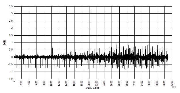
| DNL(4) | Differential nonlinearity | >–1 | LSB | |||
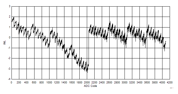
| INL(5) | Integral nonlinearity | ±3 | LSB | |||
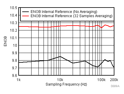
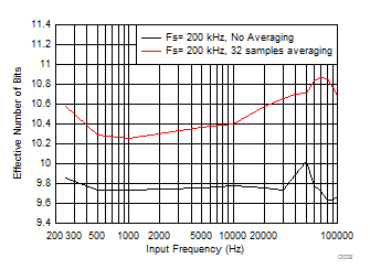
| ENOB | Effective number of bits | Internal 4.3-V equivalent reference(2), 200 ksps, 9.6-kHz input tone |
9.8 | Bits | ||
| VDDS as reference, 200 ksps, 9.6-kHz input tone | 10 | |||||
| Internal 1.44-V reference, voltage scaling disabled, 32 samples average, 200 ksps, 300-Hz input tone |
11.1 | |||||
| THD | Total harmonic distortion | Internal 4.3-V equivalent reference(2), 200 ksps, 9.6-kHz input tone |
–65 | dB | ||
| VDDS as reference, 200 ksps, 9.6-kHz input tone | –69 | |||||
| Internal 1.44-V reference, voltage scaling disabled, 32 samples average, 200 ksps, 300-Hz input tone |
–71 | |||||
| SINAD, SNDR |
Signal-to-noise and Distortion ratio |
Internal 4.3-V equivalent reference(2), 200 ksps, 9.6-kHz input tone |
60 | dB | ||
| VDDS as reference, 200 ksps, 9.6-kHz input tone | 63 | |||||
| Internal 1.44-V reference, voltage scaling disabled, 32 samples average, 200 ksps, 300-Hz input tone |
69 | |||||
| SFDR | Spurious-free dynamic range | Internal 4.3-V equivalent reference(2), 200 ksps, 9.6-kHz input tone |
67 | dB | ||
| VDDS as reference, 200 ksps, 9.6-kHz input tone | 72 | |||||
| Internal 1.44-V reference, voltage scaling disabled, 32 samples average, 200 ksps, 300-Hz input tone |
73 | |||||
| Conversion time | Serial conversion, time-to-output, 24-MHz clock | 50 | clock-cycles | |||
| Current consumption | Internal 4.3-V equivalent reference(2) | 0.66 | mA | |||
| Current consumption | VDDS as reference | 0.75 | mA | |||
| Reference voltage | Equivalent fixed internal reference (input voltage scaling enabled) | 4.3(2)(3) | V | |||
| Reference voltage | Fixed internal reference (input voltage scaling disabled) | 1.44 ±1% | V | |||
| Reference voltage | VDDS as reference (Also known as RELATIVE) (input voltage scaling enabled) | VDDS | V | |||
| Reference voltage | VDDS as reference (Also known as RELATIVE) (input voltage scaling disabled) | VDDS / 2.82(3) | V | |||
| Input Impedance | 200 ksps, voltage scaling enabled. Capacitive input, Input impedance depends on sampling frequency and sampling time | >1 | MΩ | |||
(1) Using IEEE Std
1241™-2010 for terminology and test methods.
(2) Input signal scaled down internally before conversion, as if voltage range was 0 to 4.3 V.
(3) Applied voltage must be within absolute maximum ratings (Section 5.1) at all times.
(4) No missing codes. Positive DNL typically varies from +0.3 to +3.5, depending on device (see Figure 5-24).
(5) For a typical example, see Figure 5-25.
5.15 Temperature Sensor
Measured on the TI CC2650EM-5XD reference design with Tc = 25°C, VDDS = 3.0 V, unless otherwise noted.| PARAMETER | TEST CONDITIONS | MIN | TYP | MAX | UNIT |
|---|---|---|---|---|---|
| Resolution | 4 | °C | |||
| Range | –40 | 85 | °C | ||
| Accuracy | ±5 | °C | |||
| Supply voltage coefficient(1) | 3.2 | °C/V |
(1) Automatically compensated when using supplied driver libraries.
5.16 Battery Monitor
Measured on the TI CC2650EM-5XD reference design with Tc = 25°C, VDDS = 3.0 V, unless otherwise noted.| PARAMETER | TEST CONDITIONS | MIN | TYP | MAX | UNIT |
|---|---|---|---|---|---|
| Resolution | 50 | mV | |||
| Range | 1.8 | 3.8 | V | ||
| Accuracy | 13 | mV |
5.17 Continuous Time Comparator
Tc = 25°C, VDDS = 3.0 V, unless otherwise noted.| PARAMETER | TEST CONDITIONS | MIN | TYP | MAX | UNIT |
|---|---|---|---|---|---|
| Input voltage range | 0 | VDDS | V | ||
| External reference voltage | 0 | VDDS | V | ||
| Internal reference voltage | DCOUPL as reference | 1.27 | V | ||
| Offset | 3 | mV | |||
| Hysteresis | <2 | mV | |||
| Decision time | Step from –10 mV to 10 mV | 0.72 | µs | ||
| Current consumption when enabled(1) | 8.6 | µA |
(1) Additionally, the bias module must be enabled when running in standby mode.
5.18 Low-Power Clocked Comparator
Tc = 25°C, VDDS = 3.0 V, unless otherwise noted.| PARAMETER | TEST CONDITIONS | MIN | TYP | MAX | UNIT |
|---|---|---|---|---|---|
| Input voltage range | 0 | VDDS | V | ||
| Clock frequency | 32 | kHz | |||
| Internal reference voltage, VDDS / 2 | 1.49 – 1.51 | V | |||
| Internal reference voltage, VDDS / 3 | 1.01 – 1.03 | V | |||
| Internal reference voltage, VDDS / 4 | 0.78 – 0.79 | V | |||
| Internal reference voltage, DCOUPL / 1 | 1.25 – 1.28 | V | |||
| Internal reference voltage, DCOUPL / 2 | 0.63 – 0.65 | V | |||
| Internal reference voltage, DCOUPL / 3 | 0.42 – 0.44 | V | |||
| Internal reference voltage, DCOUPL / 4 | 0.33 – 0.34 | V | |||
| Offset | <2 | mV | |||
| Hysteresis | <5 | mV | |||
| Decision time | Step from –50 mV to 50 mV | <1 | clock-cycle | ||
| Current consumption when enabled | 362 | nA |
5.19 Programmable Current Source
Tc = 25°C, VDDS = 3.0 V, unless otherwise noted.| PARAMETER | TEST CONDITIONS | MIN | TYP | MAX | UNIT |
|---|---|---|---|---|---|
| Current source programmable output range | 0.25 – 20 | µA | |||
| Resolution | 0.25 | µA | |||
| Current consumption(1) | Including current source at maximum programmable output | 23 | µA |
(1) Additionally, the bias module must be enabled when running in standby mode.
5.20 DC Characteristics
| PARAMETER | TEST CONDITIONS | MIN | TYP | MAX | UNIT |
|---|---|---|---|---|---|
| TA = 25°C, VDDS = 1.8 V | |||||
| GPIO VOH at 8-mA load | IOCURR = 2, high-drive GPIOs only | 1.32 | 1.54 | V | |
| GPIO VOL at 8-mA load | IOCURR = 2, high-drive GPIOs only | 0.26 | 0.32 | V | |
| GPIO VOH at 4-mA load | IOCURR = 1 | 1.32 | 1.58 | V | |
| GPIO VOL at 4-mA load | IOCURR = 1 | 0.21 | 0.32 | V | |
| GPIO pullup current | Input mode, pullup enabled, Vpad = 0 V | 71.7 | µA | ||
| GPIO pulldown current | Input mode, pulldown enabled, Vpad = VDDS | 21.1 | µA | ||
| GPIO high/low input transition, no hysteresis |
IH = 0, transition between reading 0 and reading 1 | 0.88 | V | ||
| GPIO low-to-high input transition, with hysteresis |
IH = 1, transition voltage for input read as 0 → 1 | 1.07 | V | ||
| GPIO high-to-low input transition, with hysteresis |
IH = 1, transition voltage for input read as 1 → 0 | 0.74 | V | ||
| GPIO input hysteresis | IH = 1, difference between 0 → 1 and 1 → 0 points | 0.33 | V | ||
| TA = 25°C, VDDS = 3.0 V | |||||
| GPIO VOH at 8-mA load | IOCURR = 2, high-drive GPIOs only | 2.68 | V | ||
| GPIO VOL at 8-mA load | IOCURR = 2, high-drive GPIOs only | 0.33 | V | ||
| GPIO VOH at 4-mA load | IOCURR = 1 | 2.72 | V | ||
| GPIO VOL at 4-mA load | IOCURR = 1 | 0.28 | V | ||
| TA = 25°C, VDDS = 3.8 V | |||||
| GPIO pullup current | Input mode, pullup enabled, Vpad = 0 V | 277 | µA | ||
| GPIO pulldown current | Input mode, pulldown enabled, Vpad = VDDS | 113 | µA | ||
| GPIO high/low input transition, no hysteresis |
IH = 0, transition between reading 0 and reading 1 | 1.67 | V | ||
| GPIO low-to-high input transition, with hysteresis |
IH = 1, transition voltage for input read as 0 → 1 | 1.94 | V | ||
| GPIO high-to-low input transition, with hysteresis |
IH = 1, transition voltage for input read as 1 → 0 | 1.54 | V | ||
| GPIO input hysteresis | IH = 1, difference between 0 → 1 and 1 → 0 points | 0.4 | V | ||
| TA = 25°C | |||||
| VIH | Lowest GPIO input voltage reliably interpreted as a «High» | 0.8 | VDDS(1) | ||
| VIL | Highest GPIO input voltage reliably interpreted as a «Low» | 0.2 | VDDS(1) | ||
(1) Each GPIO is referenced to a specific VDDS pin. See the technical reference manual listed in Section 8.2 for more details.
5.21 Thermal Characteristics
| NAME | DESCRIPTION | RSM (°C/W)(1)(2) | RHB (°C/W)(1)(2) | RGZ (°C/W)(1)(2) |
|---|---|---|---|---|
| RθJA | Junction-to-ambient thermal resistance | 36.9 | 32.8 | 29.6 |
| RθJC(top) | Junction-to-case (top) thermal resistance | 30.3 | 24.0 | 15.7 |
| RθJB | Junction-to-board thermal resistance | 7.6 | 6.8 | 6.2 |
| PsiJT | Junction-to-top characterization parameter | 0.4 | 0.3 | 0.3 |
| PsiJB | Junction-to-board characterization parameter | 7.4 | 6.8 | 6.2 |
| RθJC(bot) | Junction-to-case (bottom) thermal resistance | 2.1 | 1.9 | 1.9 |
(1) °C/W = degrees Celsius per watt.
(2) These values are based on a JEDEC-defined 2S2P system (with the exception of the Theta JC [RθJC] value, which is based on a JEDEC-defined 1S0P system) and will change based on environment as well as application. For more information, see these EIA/JEDEC standards:
- JESD51-2, Integrated Circuits Thermal Test Method Environmental Conditions - Natural Convection (Still Air).
- JESD51-3, Low Effective Thermal Conductivity Test Board for Leaded Surface Mount Packages.
- JESD51-7, High Effective Thermal Conductivity Test Board for Leaded Surface Mount Packages.
- JESD51-9, Test Boards for Area Array Surface Mount Package Thermal Measurements.
5.22 Timing Requirements
| MIN | NOM | MAX | UNIT | |||
|---|---|---|---|---|---|---|
| Rising supply-voltage slew rate | 0 | 100 | mV/µs | |||
| Falling supply-voltage slew rate | 0 | 20 | mV/µs | |||
| Falling supply-voltage slew rate, with low-power flash settings(1) | 3 | mV/µs | ||||
| Positive temperature gradient in standby(3) | No limitation for negative temperature gradient, or outside standby mode | 5 | °C/s | |||
| CONTROL INPUT AC CHARACTERISTICS(2) | ||||||
| RESET_N low duration | 1 | µs | ||||
| SYNCHRONOUS SERIAL INTERFACE (SSI) (4) | ||||||
| S1 (SLAVE) (5) | tclk_per | SSIClk period | 12 | 65024 | system clocks | |
| S2 (5) | tclk_high | SSIClk high time | 0.5 | tclk_per | ||
| S3(5) | tclk_low | SSIClk low time | 0.5 | tclk_per | ||
(1) For smaller coin cell batteries, with high worst-case end-of-life equivalent source resistance, a 22-µF VDDS input capacitor (see Figure 7-1) must be used to ensure compliance with this slew rate.
(2) TA = –40°C to 85°C, VDDS = 1.7 V to 3.8 V, unless otherwise noted.
(3) Applications using RCOSC_LF as sleep timer must also consider the drift in frequency caused by a change in temperature (see Section 5.13).
(4) Tc = 25°C, VDDS = 3.0 V, unless otherwise noted. Device operating as SLAVE. For SSI MASTER operation, see Section 5.23.
5.23 Switching Characteristics
Measured on the TI CC2650EM-5XD reference design with Tc = 25°C, VDDS = 3.0 V, unless otherwise noted.| PARAMETER | TEST CONDITIONS | MIN | TYP | MAX | UNIT | |
|---|---|---|---|---|---|---|
| WAKEUP AND TIMING | ||||||
| Idle → Active | 14 | µs | ||||
| Standby → Active | 151 | µs | ||||
| Shutdown → Active | 1015 | µs | ||||
| SYNCHRONOUS SERIAL INTERFACE (SSI) (1) | ||||||
| S1 (TX only)(2) tclk_per (SSIClk period) | One-way communication to SLAVE | 4 | 65024 | system clocks | ||
| S1 (TX and RX)(2) tclk_per (SSIClk period) | Normal duplex operation | 8 | 65024 | system clocks | ||
| S2 (2) tclk_high (SSIClk high time) | 0.5 | tclk_per | ||||
| S3 (2) tclk_low(SSIClk low time) | 0.5 | tclk_per | ||||
(1) Device operating as MASTER. For SSI SLAVE operation, see Section 5.22.
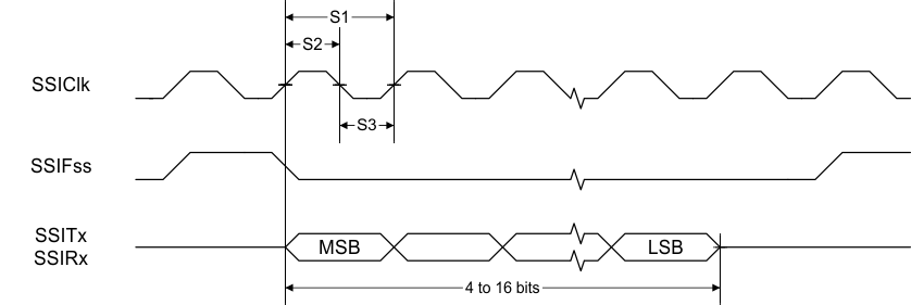 Figure 5-1 SSI Timing for TI Frame Format (FRF = 01), Single Transfer Timing Measurement
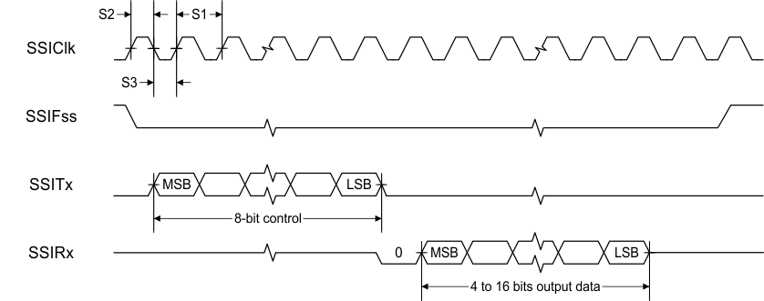 Figure 5-2 SSI Timing for MICROWIRE Frame Format (FRF = 10), Single Transfer
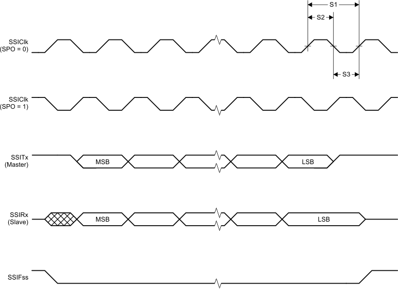 Figure 5-3 SSI Timing for SPI Frame Format (FRF = 00), With SPH = 1
5.24 Typical Characteristics
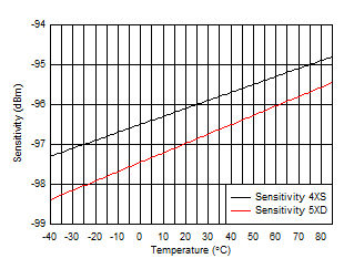
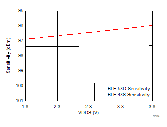
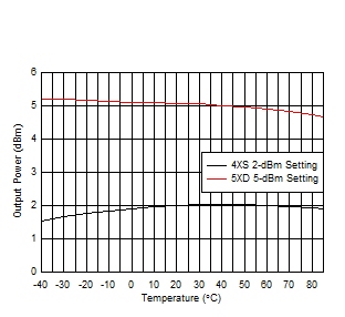
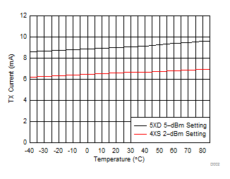
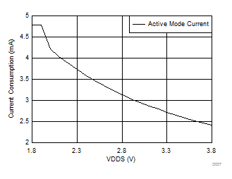
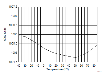
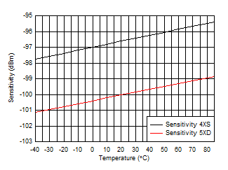
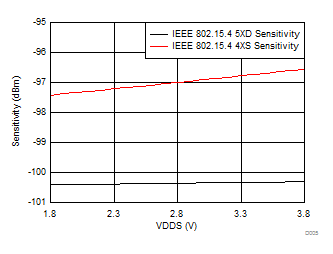
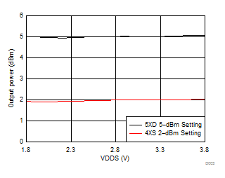
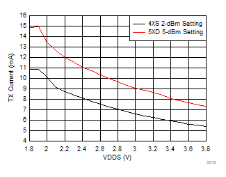
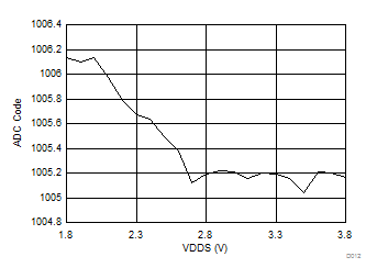
vs Supply Voltage (VDDS)
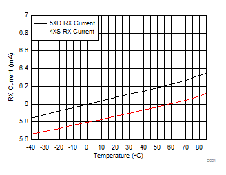
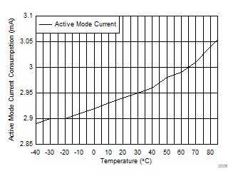
Current Consumption vs Temperature
