ZHCSAN2E december   2012  – april 2021 BQ7716

PRODUCTION DATA  

  1.   1
  2. 特性
  3. 应用
  4. 说明
  5. Revision History
  6. Device Comparison Table
  7. Pin Configuration and Functions
  8. Specifications
    1. 7.1 Absolute Maximum Ratings
    2. 7.2 ESD Ratings
    3. 7.3 Recommended Operating Conditions
    4. 7.4 Thermal Information
    5. 7.5 Electrical Characteristics
    6. 7.6 Typical Characteristics
  9. Detailed Description
    1. 8.1 Overview
    2. 8.2 Functional Block Diagram
    3. 8.3 Feature Description
      1. 8.3.1 Sense Positive Input for Vx
      2. 8.3.2 Output Drive, OUT
      3. 8.3.3 Supply Input, VDD
      4. 8.3.4 External Delay Capacitor, CD
    4. 8.4 Device Functional Modes
      1. 8.4.1 NORMAL Mode
      2. 8.4.2 OVERVOLTAGE Mode
      3. 8.4.3 Customer Test Mode
  10. Application and Implementation
    1. 9.1 Application Information
    2. 9.2 Typical Application
      1. 9.2.1 Design Requirements
      2. 9.2.2 Detailed Design Procedure
      3. 9.2.3 Application Curves
  11. 10Power Supply Recommendations
  12. 11Layout
    1. 11.1 Layout Guidelines
    2. 11.2 Layout Example
  13. 12Device and Documentation Support
    1. 12.1 Receiving Notification of Documentation Updates
    2. 12.2 支持资源
    3. 12.3 Trademarks
    4. 12.4 静电放电警告
    5. 12.5 Export Control Notice
    6. 12.6 术语表
  14. 13Mechanical, Packaging, and Orderable Information

封装选项

机械数据 (封装 | 引脚)
散热焊盘机械数据 (封装 | 引脚)
订购信息

Application Information

Figure 9-1 shows each external component.
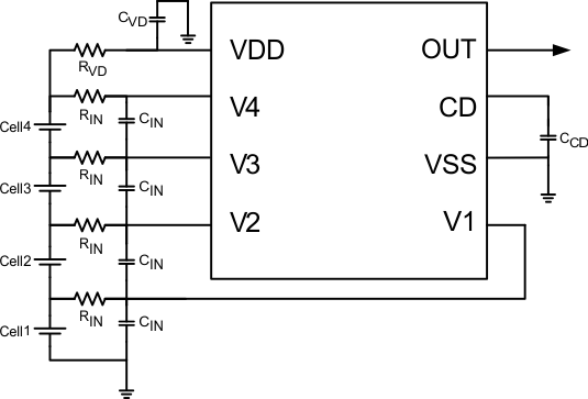
GUID-8972C5A9-E41F-4CE8-8758-D85CC0692BF5-low.gifFigure 9-1 Application Configuration
Note:

In the case of an Open Drain Active Low configuration, an external pull-up resistor is required on the OUT terminal.

Changes to the ranges stated in Table 9-1 will impact the accuracy of the cell measurements.

Note:

The device is calibrated using an RIN value = 1 kΩ. Using a value other than this recommended value changes the accuracy of the cell voltage measurements and VOV trigger level.