ZHCSM89 july 2021 BQ51013B-Q1
PRODUCTION DATA
- 1
- 1 特性
- 2 应用
- 3 说明
- 4 Revision History
- 5 Description (continued)
- 6 Device Comparison Table
- 7 Pin Configuration and Functions
- 8 Specifications
-
9 Detailed Description
- 9.1 Overview
- 9.2 Functional Block Diagram
- 9.3
Feature Description
- 9.3.1 Details of a Qi Wireless Power System and BQ51013B-Q1 Power Transfer Flow Diagrams
- 9.3.2 Dynamic Rectifier Control
- 9.3.3 Dynamic Efficiency Scaling
- 9.3.4 RILIM Calculations
- 9.3.5 Input Overvoltage
- 9.3.6 Adapter Enable Functionality and EN1/EN2 Control
- 9.3.7 End Power Transfer Packet (WPC Header 0x02)
- 9.3.8 Status Outputs
- 9.3.9 WPC Communication Scheme
- 9.3.10 Communication Modulator
- 9.3.11 Adaptive Communication Limit
- 9.3.12 Synchronous Rectification
- 9.3.13 Temperature Sense Resistor Network (TS)
- 9.3.14 3-State Driver Recommendations for the TS/CTRL Pin
- 9.3.15 Thermal Protection
- 9.3.16 WPC v1.2 Compliance – Foreign Object Detection
- 9.3.17 Receiver Coil Load-Line Analysis
- 9.4 Device Functional Modes
-
10Application and Implementation
- 10.1 Application Information
- 10.2
Typical Applications
- 10.2.1
BQ51013B-Q1 Wireless Power Receiver Used as a Power
Supply
- 10.2.1.1 Design Requirements
- 10.2.1.2
Detailed Design Procedure
- 10.2.1.2.1 Using The BQ51013B-Q1 as a Wireless Power Supply: (See )
- 10.2.1.2.2 Series and Parallel Resonant Capacitor Selection
- 10.2.1.2.3 Recommended RX Coils
- 10.2.1.2.4 COMM, CLAMP, and BOOT Capacitors
- 10.2.1.2.5 Control Pins and CHG
- 10.2.1.2.6 Current Limit and FOD
- 10.2.1.2.7 RECT and OUT Capacitance
- 10.2.1.3 Application Curves
- 10.2.2 Dual Power Path: Wireless Power and DC Input
- 10.2.3 Wireless and Direct Charging of a Li-Ion Battery at 800 mA
- 10.2.1
BQ51013B-Q1 Wireless Power Receiver Used as a Power
Supply
- 11Power Supply Recommendations
- 12Layout
- 13Device and Documentation Support
- 14Mechanical, Packaging, and Orderable Information
9.3.13 Temperature Sense Resistor Network (TS)
The BQ51013B-Q1 includes a ratiometric external temperature sense function. The temperature sense function has two ratiometric thresholds which represent a hot and cold condition. An external temperature sensor is recommended in order to provide safe operating conditions for the receiver product. This pin is best used for monitoring the surface that can be exposed to the end user (place the NTC resistor closest to where the user would physically contact the end product).
Figure 9-12 allows for any NTC resistor to be used with the given VHOT and VCOLD thresholds.
 Figure 9-12 NTC Circuit Options For Safe Operation of the Wireless Receiver Power Supply
The resistors R1 and R3 can be solved by resolving the system of equations at the desired temperature thresholds. The two equations are:
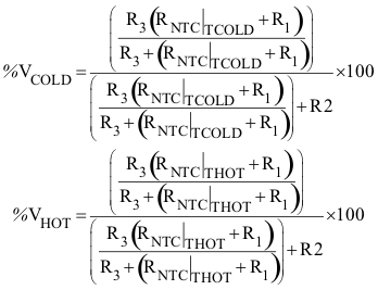
Where:
where
- TCOLD and THOT are the desired temperature thresholds in degrees Kelvin.
- RO is the nominal resistance.
- β is the temperature coefficient of the NTC resistor.
R2 is fixed at 20 kΩ. An example solution is provided:
- R1 = 4.23 kΩ
- R3 = 66.8 kΩ
where the chosen parameters are:
- %VHOT = 19.6%
- %VCOLD = 58.7%
- TCOLD = –10°C
- THOT = 100°C
- β = 3380
- RO = 10 kΩ
The plot of the percent VTSB vs. temperature is shown in Figure 9-13:
 Figure 9-13 Example Solution for an NTC Resistor with RO = 10 kΩ and β = 3380
Figure 9-14 illustrates the periodic biasing scheme used for measuring the TS state. An internal TS_READ signal enables the TS bias voltage (VTS-Bias) for 24 ms. During this period, the TS comparators are read (with tTS deglitch) and appropriate action is taken based on the temperature measurement. After this 24-ms period has elapsed, the TS_READ signal goes low, which causes the TS/CTRL pin to become high impedance. During the next 35 ms (priority packet period) or 235 ms (standard packet period), the TS voltage is monitored and compared to VCTRL-HI. If the TS voltage is greater than VCTRL-HI then a secondary device is driving the TS/CTRL pin and a CTRL = ‘1’ is detected.
 Figure 9-14 Timing Diagram For TS Detection Circuit