SLUSA96B August   2010  – April 2016 BQ32002

PRODUCTION DATA.  

  1. Features
  2. Applications
  3. Description
  4. Revision History
  5. Pin Configuration and Functions
  6. Specifications
    1. 6.1 Absolute Maximum Ratings
    2. 6.2 ESD Ratings
    3. 6.3 Recommended Operating Conditions
    4. 6.4 Thermal Information
    5. 6.5 Electrical Characteristics
    6. 6.6 Timing Requirements
    7. 6.7 Typical Characteristics
  7. Detailed Description
    1. 7.1 Overview
    2. 7.2 Functional Block Diagram
    3. 7.3 Feature Description
      1. 7.3.1 IRQ Function
      2. 7.3.2 VBACK Switchover
    4. 7.4 Device Functional Modes
    5. 7.5 Programming
      1. 7.5.1 I2C Serial Interface
    6. 7.6 Register Maps
      1. 7.6.1 I2C Read After Backup Mode
      2. 7.6.2 Normal Register Descriptions
      3. 7.6.3 Special Function Registers
  8. Application and Implementation
    1. 8.1 Application Information
    2. 8.2 Typical Application
      1. 8.2.1 Design Requirements
      2. 8.2.2 Detailed Design Procedure
        1. 8.2.2.1 Reading From a Register
        2. 8.2.2.2 Leap Year Compensation
        3. 8.2.2.3 Utilizing the Backup Supply
      3. 8.2.3 Application Curves
  9. Power Supply Recommendations
  10. 10Layout
    1. 10.1 Layout Guidelines
    2. 10.2 Layout Example
  11. 11Device and Documentation Support
    1. 11.1 Community Resources
    2. 11.2 Trademarks
    3. 11.3 Electrostatic Discharge Caution
    4. 11.4 Glossary
  12. 12Mechanical, Packaging, and Orderable Information

封装选项

机械数据 (封装 | 引脚)
散热焊盘机械数据 (封装 | 引脚)
订购信息

5 Pin Configuration and Functions

D Package
8-Pin SOIC
Top View
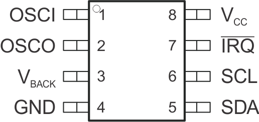
BQ32002 pinout_d8_lus900.gif

Pin Functions

PIN TYPE DESCRIPTION
NAME NO.
POWER AND GROUND
VCC 8 Main device power
GND 4 Ground
VBACK 3 Backup device power
SERIAL INTERFACE
SCL 6 I I2C serial interface clock
SDA 5 I/O I2C serial data
INTERRUPT
IRQ 7 O Configurable interrupt output. Open-drain output.
OSCILLATOR
OSCI 1 Oscillator input
OSCO 2 Oscillator output