ZHCSB26A May 2013 – August 2014
PRODUCTION DATA.
- 1 特性
- 2 应用
- 3 说明
- 4 简化电路原理图
- 5 修订历史记录
- 6 Device Comparison Table
- 7 Pin Configuration and Functions
-
8 Specifications
- 8.1 Absolute Maximum Ratings
- 8.2 Handling Ratings
- 8.3 Recommended Operating Conditions
- 8.4 Thermal Information
- 8.5 Supply Current
- 8.6 Digital Input and Output DC Characteristics
- 8.7 LDO Regulator, Wake-up, and Auto-shutdown DC Characteristics
- 8.8 ADC (Temperature and Cell Measurement) Characteristics
- 8.9 Integrating ADC (Coulomb Counter) Characteristics
- 8.10 Integrated Sense Resistor Characteristics
- 8.11 I2C-Compatible Interface Communication Timing Characteristics
- 9 Detailed Description
- 10Application and Implementation
- 11Power Supply Recommendation
- 12Layout
- 13器件和文档支持
- 14机械封装和可订购信息
7 Pin Configuration and Functions
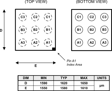
Pin Functions
| PIN | TYPE(1) | DESCRIPTION | |
|---|---|---|---|
| NAME | NUMBER | ||
| BAT | C3 | PI, AI | LDO regulator input, battery voltage input, and coulomb counter input typically connected to the PACK+ terminal. |
| BIN | B1 | DI | Battery insertion detection input. If Operation Configuration bit [BIE] = 1 (default), a logic low on the pin is detected as battery insertion. For a removable pack, the BIN pin can be connected to VSS through a pulldown resistor on the pack, typically the 10-kΩ thermistor; the system board should use a 1.8-MΩ pullup resistor to VDD to ensure the BIN pin is high when a battery is removed. If the battery is embedded in the system, it is recommended to leave [BIE] = 1 and use a 10-kΩ pulldown resistor from BIN to VSS. If [BIE] = 0, then the host must inform the gauge of battery insertion and removal with the BAT_INSERT and BAT_REMOVE subcommands. A 10-kΩ pulldown resistor should be placed between BIN and VSS, even if this pin is unused. NOTE: The BIN pin must not be shorted directly to VCC or VSS and any pullup resistor on the BIN pin must be connected only to VDD and not an external voltage rail. |
| GPOUT | A1 | DO | This open-drain output can be configured to indicate BAT_LOW when the Operation Configuration[BATLOWEN] bit is set. By default [BATLOWEN] is cleared and this pin performs an interrupt function (SOC_INT) by pulsing for specific events, such as a change in State of Charge. Signal polarity for these functions is controlled by the [GPIOPOL] configuration bit. This pin should not be left floating, even if unused, so a 10-kΩ pullup resistor is recommended. |
| SCL | A3 | DIO | Slave I2C serial bus for communication with system (Master). Open-drain pins. Use with external 10-kΩ pullup resistors (typical) for each pin. If the external pullup resistors will be disconnected from these pins during normal operation, recommend using external 1-MΩ pulldown resistors to VSS at each pin to avoid floating inputs. |
| SDA | A2 | DIO | |
| SRX | C2 | AI | Integrated high-side sense resistor and coulomb counter input typically connected to system power rail VSYS. |
| VDD | B3 | PO | 1.8-V Regulator Output. Decouple with 0.47-μF ceramic capacitor to VSS. This pin is not intended to provide power for other devices in the system. |
| VSS | B2, C1 | PI | Ground pins. The center pin B2 is the actual device ground pin while pin C1 is floating internally and therefore C1 may be used as a bridge to connect to the board ground plane without requiring a via under the device package. Recommend routing the center pin B2 to the corner pin C1 using a top-layer metal trace on the board. Then route the corner pin C1 to the board ground plane. |
(1) IO = Digital input-output, AI = Analog input, P = Power connection