ZHCSB26A May 2013 – August 2014
PRODUCTION DATA.
- 1 特性
- 2 应用
- 3 说明
- 4 简化电路原理图
- 5 修订历史记录
- 6 Device Comparison Table
- 7 Pin Configuration and Functions
-
8 Specifications
- 8.1 Absolute Maximum Ratings
- 8.2 Handling Ratings
- 8.3 Recommended Operating Conditions
- 8.4 Thermal Information
- 8.5 Supply Current
- 8.6 Digital Input and Output DC Characteristics
- 8.7 LDO Regulator, Wake-up, and Auto-shutdown DC Characteristics
- 8.8 ADC (Temperature and Cell Measurement) Characteristics
- 8.9 Integrating ADC (Coulomb Counter) Characteristics
- 8.10 Integrated Sense Resistor Characteristics
- 8.11 I2C-Compatible Interface Communication Timing Characteristics
- 9 Detailed Description
- 10Application and Implementation
- 11Power Supply Recommendation
- 12Layout
- 13器件和文档支持
- 14机械封装和可订购信息
12 Layout
12.1 Layout Guidelines
- A capacitor, of value at least 0.47 µF, is connected between the VDD pin and VSS. The capacitor should be placed close to the gauge IC and have short traces to both the VDD pin and VSS.
- It is recommend to have a capacitor, at least 1.0 µF, connect between the BAT pin and VSS if the connection between the battery pack and the gauge BAT pin has the potential to pick up noise. The capacitor should be placed close to the gauge IC and have short traces to both the VDD pin and VSS.
- If the external pullup resistors on the SCL and SDA lines will be disconnected from the host during low-power operation, it is recommend to use external 1-MΩ pulldown resistors to VSS to avoid floating inputs to the I2C engine.
- The value of the SCL and SDA pullup resistors should take into consideration the pullup voltage and the bus capacitance. Some recommended values, assuming a bus capacitance of 10 pF, can be seen in Table 4.
- If the GPOUT pin is not used by the host, the pin should still be pulled up to VDD with a 4.7-kΩ or 10-kΩ resistor.
- If the battery pack thermistor is not connected to the BIN pin, the BIN pin should be pulled down to VSS with a 10-kΩ resistor.
- The BIN pin should not be shorted directly to VDD or VSS.
- The actual device ground is the center pin (B2). The C1 pin is floating internally and can be used as a bridge to connect the board ground plane to the device ground (B2).
Table 4. Recommended Values for SCL and SDA Pullup Resistors
| VPU | 1.8 V | 3.3 V | ||
|---|---|---|---|---|
| RPU | Range | Typical | Range | Typical |
| 400 Ω ≤ RPU ≤ 37.6 kΩ | 10 kΩ | 900 Ω ≤ RPU ≤ 29.2 kΩ | 5.1 kΩ | |
12.2 Layout Example
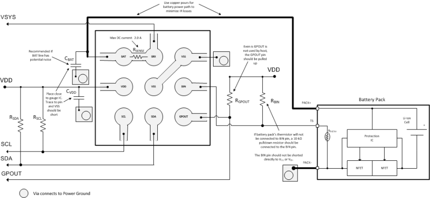 Figure 2. bq27421-G1 Board Layout