ZHCSGR7 September 2017
PRODUCTION DATA.
- 1 特性
- 2 应用
- 3 说明
- 4 修订历史记录
- 5 说明 (续)
- 6 Pin Configuration and Functions
- 7 Specifications
-
8 Detailed Description
- 8.1 Overview
- 8.2 Functional Block Diagram
- 8.3
Feature Description
- 8.3.1 Power-On-Reset (POR)
- 8.3.2 Device Power Up from Battery without Input Source
- 8.3.3 Power Up from Input Source
- 8.3.4 Host Mode and Standalone Power Management
- 8.3.5 Power Path Management
- 8.3.6 Battery Charging Management
- 8.3.7 Shipping Mode
- 8.3.8 Status Outputs (PG, STAT)
- 8.3.9 Protections
- 8.3.10 Serial interface
- 8.4 Register Maps
- 9 Application and Implementation
- 10Power Supply Recommendations
- 11Layout
- 12器件和文档支持
- 13机械、封装和可订购信息
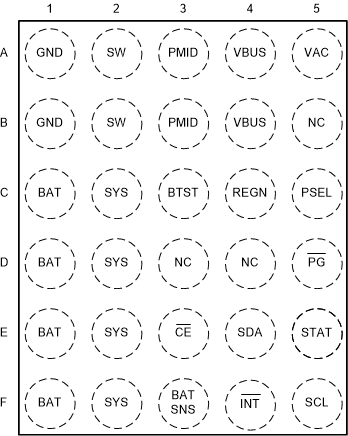
6 Pin Configuration and Functions
bq25600C YFF Package
30-Pin DSBGA
Top View

Pin Functions
| PIN | TYPE(1) | DESCRIPTION | |
|---|---|---|---|
| NAME | NO. | ||
| NC | B5 | AO | No Connect. Must leave this pin floating. |
| BAT | C1 | P | Battery connection point to the positive terminal of the battery pack. The internal current sensing resistor is connected between SYS and BAT. Connect a 10 µF closely to the BAT pin. |
| D1 | |||
| E1 | |||
| F1 | |||
| BATSNS | F3 | AIO | Battery voltage sensing pin for charge current regulation. in order to minimize the parasitic trace resistance during charging, BATSNS pin is connected to the actual battery pack as close as possible. |
| BTST | C3 | P | PWM high side driver positive supply. internally, the BTST is connected to the cathode of the boost-strap diode. Connect the 0.047-μF bootstrap capacitor from SW to BTST. |
| CE | E3 | DI | Charge enable pin. When this pin is driven low, battery charging is enabled. |
| GND | A1 | — | |
| B1 | |||
| INT | F4 | DO | Open-drain interrupt Output. Connect the INT to a logic rail through 10-kΩ resistor. The INT pin sends active low, 256-µs pulse to host to report charger device status and fault. |
| PG | D5 | DO | Open drain active low power good indicator. Connect to the pull up rail through 10 kΩ resistor. LOW indicates a good input source if the input voltage is between UVLO and ACOV, above SLEEP mode threshold, and current limit is above 30 mA. |
| PMID | A3 | DO | Connected to the drain of the reverse blocking MOSFET (RBFET) and the drain of HSFET. Given the total input capacitance, put 1 μF on VBUS to GND, and the rest capacitance on PMID to GND. |
| B3 | |||
| PSEL | C5 | DI | Power source selection input. High indicates 500 mA input current limit. Low indicates 2.4A input current limit. Once the device gets into host mode, the host can program different input current limit to IINDPM register. |
| REGN | C4 | P | PWM low side driver positive supply output. internally, REGN is connected to the anode of the boost-strap diode. Connect a 4.7-μF (10-V rating) ceramic capacitor from REGN to analog GND. The capacitor should be placed close to the IC. |
| SCL | F5 | DI | I2C interface clock. Connect SCL to the logic rail through a 10-kΩ resistor. |
| SDA | E4 | DIO | I2C interface data. Connect SDA to the logic rail through a 10-kΩ resistor. |
| STAT | E5 | DO | Open-drain interrupt output. Connect the STAT pin to a logic rail via 10-kΩ resistor. The STAT pin indicates charger status. Charge in progress: LOW Charge complete or charger in SLEEP mode: HIGH Charge suspend (fault response): Blink at 1Hz |
| SW | A2 | P | Switching node connecting to output inductor. Internally SW is connected to the source of the n-channel HSFET and the drain of the n-channel LSFET. Connect the 0.047-μF bootstrap capacitor from SW to BTST. |
| B2 | |||
| SYS | C2 | P | Converter output connection point. The internal current sensing resistor is connected between SYS and BAT. Connect a 20 µF closely to the SYS pin. |
| D2 | |||
| E2 | |||
| F2 | |||
| Thermal Pad | — | P | Ground reference for the device that is also the thermal pad used to conduct heat from the device. This connection serves two purposes. The first purpose is to provide an electrical ground connection for the device. The second purpose is to provide a low thermal-impedance path from the device die to the PCB. This pad should be tied externally to a ground plane. |
| NC | D3, D4 | AI | No Connect. Leave this pin floating. |
| VAC | A5 | AI | Input voltage sensing. This pin must be connected to VBUS. |
| VBUS | A4 | P | Charger input voltage. The internal n-channel reverse block MOSFET (RBFET) is connected between VBUS and PMID with VBUS on source. Place a 1-uF ceramic capacitor from VBUS to GND and place it as close as possible to IC. |
| B4 | |||
(1) AI = Analog input, AO = Analog Output, AIO = Analog input Output, DI = Digital input, DO = Digital Output, DIO = Digital input Output, P = Power