ZHCSGR7 September   2017

PRODUCTION DATA.  

  1. 特性
  2. 应用
  3. 说明
  4. 修订历史记录
  5. 说明 (续)
  6. Pin Configuration and Functions
  7. Specifications
    1. 7.1 Absolute Maximum Ratings
    2. 7.2 ESD Ratings
    3. 7.3 Recommended Operating Conditions
    4. 7.4 Thermal information
    5. 7.5 Electrical Characteristics
    6. 7.6 Timing Requirements
    7. 7.7 Typical Characteristics
  8. Detailed Description
    1. 8.1 Overview
    2. 8.2 Functional Block Diagram
    3. 8.3 Feature Description
      1. 8.3.1  Power-On-Reset (POR)
      2. 8.3.2  Device Power Up from Battery without Input Source
      3. 8.3.3  Power Up from Input Source
        1. 8.3.3.1 Power Up REGN Regulation
        2. 8.3.3.2 Poor Source Qualification
        3. 8.3.3.3 Input Source Type Detection
          1. 8.3.3.3.1 PSEL Pins Sets Input Current Limit in bq25600C
        4. 8.3.3.4 Input Voltage Limit Threshold Setting (VINDPM Threshold)
        5. 8.3.3.5 Converter Power-Up
      4. 8.3.4  Host Mode and Standalone Power Management
        1. 8.3.4.1 Host Mode and Default Mode in bq25600C
      5. 8.3.5  Power Path Management
      6. 8.3.6  Battery Charging Management
        1. 8.3.6.1 Autonomous Charging Cycle
        2. 8.3.6.2 Battery Charging Profile
        3. 8.3.6.3 Charging Termination
        4. 8.3.6.4 Charging Safety Timer
        5. 8.3.6.5 Narrow VDC Architecture
      7. 8.3.7  Shipping Mode
        1. 8.3.7.1 BATFET Disable Mode (Shipping Mode)
        2. 8.3.7.2 BATFET Enable (Exit Shipping Mode)
      8. 8.3.8  Status Outputs (PG, STAT)
        1. 8.3.8.1 Power Good indicator (PG Pin and PG_STAT Bit)
        2. 8.3.8.2 Charging Status indicator (STAT)
        3. 8.3.8.3 Interrupt to Host (INT)
      9. 8.3.9  Protections
        1. 8.3.9.1 Voltage and Current Monitoring in Converter Operation
          1. 8.3.9.1.1 Voltage and Current Monitoring in Buck Mode
            1. 8.3.9.1.1.1 Input Overvoltage (ACOV)
        2. 8.3.9.2 Thermal Regulation and Thermal Shutdown
          1. 8.3.9.2.1 Thermal Protection in Buck Mode
        3. 8.3.9.3 Battery Protection
          1. 8.3.9.3.1 Battery overvoltage Protection (BATOVP)
      10. 8.3.10 Serial interface
        1. 8.3.10.1 Data Validity
        2. 8.3.10.2 START and STOP Conditions
        3. 8.3.10.3 Byte Format
        4. 8.3.10.4 Acknowledge (ACK) and Not Acknowledge (NACK)
        5. 8.3.10.5 Slave Address and Data Direction Bit
        6. 8.3.10.6 Single Read and Write
        7. 8.3.10.7 Multi-Read and Multi-Write
    4. 8.4 Register Maps
      1. 8.4.1  REG00
      2. 8.4.2  REG01
      3. 8.4.3  REG02
      4. 8.4.4  REG03
      5. 8.4.5  REG04
      6. 8.4.6  REG05
      7. 8.4.7  REG06
      8. 8.4.8  REG07
      9. 8.4.9  REG08
      10. 8.4.10 REG09
      11. 8.4.11 REG0A
      12. 8.4.12 REG0B
  9. Application and Implementation
    1. 9.1 Application information
    2. 9.2 Typical Application Diagram
      1. 9.2.1 Design Requirements
      2. 9.2.2 Detailed Design Procedure
        1. 9.2.2.1 Inductor Selection
        2. 9.2.2.2 input Capacitor
        3. 9.2.2.3 Output Capacitor
    3. 9.3 Application Curves
  10. 10Power Supply Recommendations
  11. 11Layout
    1. 11.1 Layout Guidelines
    2. 11.2 Layout Example
  12. 12器件和文档支持
    1. 12.1 社区资源
    2. 12.2 商标
    3. 12.3 静电放电警告
    4. 12.4 Glossary
  13. 13机械、封装和可订购信息

封装选项

机械数据 (封装 | 引脚)
散热焊盘机械数据 (封装 | 引脚)
订购信息

Layout

Layout Guidelines

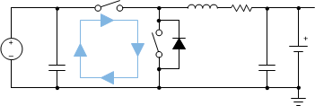
The switching node rise and fall times should be minimized for minimum switching loss. Proper layout of the components to minimize high frequency current path loop (see Figure 29) is important to prevent electrical andmagnetic field radiation and high frequency resonant problems.

IMPORTANT

It is essential to follow this specific layout PCB order.

  • Place input capacitor as close as possible to PMID pin and GND pin connections and use shortest copper trace connection or GND plane.
  • Put output capacitor near to the inductor and the device.
  • Decoupling capacitors should be placed next to the device pins and make trace connection as short as possible.
  • Place inductor input terminal to SW pin as close as possible. Minimize the copper area of this trace to lower electrical and magnetic field radiation but make the trace wide enough to carry the charging current. Do not use multiple layers in parallel for this connection. Minimize parasitic capacitance from this area to any other trace or plane.
  • It is OK to connect all grounds together to reduce PCB size and improve thermal dissipation.
  • Try to avoid ground planes in parallel with high frequency traces in other layers.
  • See the EVM design for the recommended component placement with trace and via locations.

Layout Example

bq25600C High_Frequency_Current_Path_SLUSCJ4.gif Figure 29. High Frequency Current Path