ZHCSMW0 October 2021 BQ25170J
PRODUCTION DATA
- 1 特性
- 2 应用
- 3 说明
- 4 Revision History
- 5 Pin Configuration and Functions
- 6 Specifications
- 7 Detailed Description
- 8 Application and Implementation
- 9 Power Supply Recommendations
- 10Layout
- 11Device and Documentation Support
- 12Mechanical, Packaging, and Orderable Information
7.3.2.4 Battery Temperature Qualification (TS Pin)
While charging, the device continuously monitors battery temperature by sensing the voltage at the TS pin. A negative temperature coefficient (NTC) thermistor should be connected between the TS and GND pins (recommend: 103AT-2). If temperature sensing is not required in the application, connect a fixed 10-kΩ resistor from TS to GND to allow normal operation.
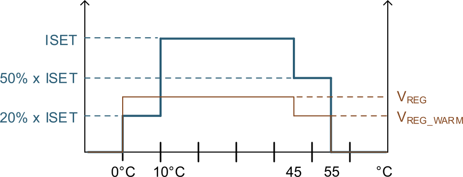
The TS function for BQ25170J is designed to follow the JEITA temperature standard for Li-Ion and Li-Poly batteries; charge current (ISET) and regulation voltage (VREG) are reduced based on battery temp (TS). There are four thresholds, Hot-55C, Warm-45C, Cool-10C and Cold-0C.
Normal operation occurs between 10C and 45C, charge current and voltage will be the normal values. When battery is in the Cool temperature range, between 0C and 10C, the charger current level is 20% of ISET value and regulation voltage is not changed. When the battery is in the Warm temperature range, between 45C and 55C, ISET is reduced by 50% and regulation voltage is reduced to 4.1V for VSET settings greater than 4.1V. Regulation voltage is not reduced during the Warm region for VSET settings less than or equal to 4.1V. Charge is suspended below Cold temp of 0C and above Hot temp of 55C. When charge is suspended device enters the STANDBY state, and blinks the STAT pin. Once battery temperature returns to normal conditions, charging resumes automatically. See Figure 7-3.
When charge current is reduced during Cool or Warm temp the safety timer runs at half the clock rate.
 Figure 7-3 Standard JEITA Profile figure
In addition to battery temperature sensing, the TS pin can be used to disable the charger at any time by pulling TS voltage below VTS_ENZ. The device disables the charger and consumes ISD_IN_TS from the input supply. In order to minimize quiescent current, the TS current source (ITS_BIAS) is duty-cycled, with an on-time of tTS_DUTY_ON and an off time of tTS_DUTY_OFF. After the TS pin pull-down is released, the device may take up to tTS_DUTY_OFF to turn the ITS_BIAS back on. After the source is turned on, the TS pin voltage will go above VTS_EN, and re-enable the charger operation. The device treats this TS pin toggle as an input supply toggle, triggering Device Power Up From Input Source (Section 7.3.1).