SLUS891B February 2010 – November 2014
PRODUCTION DATA.
- 1 Features
- 2 Applications
- 3 Description
- 4 Revision History
- 5 Pin Configuration and Functions
- 6 Specifications
-
7 Detailed Description
- 7.1 Overview
- 7.2 Functional Block Diagram
- 7.3
Feature Description
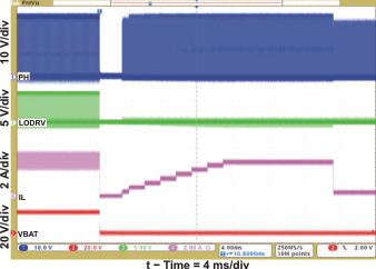
- 7.3.1 Battery Voltage Regulation
- 7.3.2 Battery Current Regulation
- 7.3.3 Precharge
- 7.3.4 Charge Termination, Recharge, and Safety Timer
- 7.3.5 Power Up
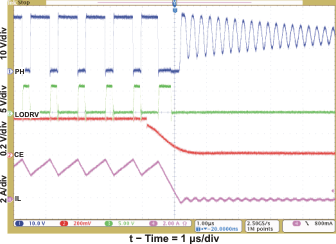
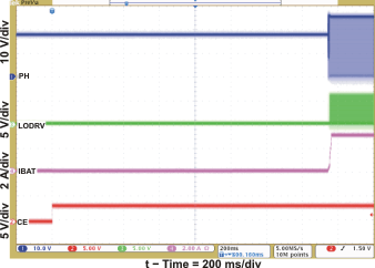
- 7.3.6 Enable and Disable Charging
- 7.3.7 Automatic Internal Soft-Start Charger Current
- 7.3.8 Cycle-by-Cycle Charge Undercurrent Protection
- 7.3.9 Input Overvoltage Protection (ACOV)
- 7.3.10 Input Undervoltage Lock-Out (UVLO)
- 7.3.11 Battery Overvoltage Protection
- 7.3.12 Cycle-by-Cycle Charge Overcurrent Protection
- 7.3.13 Thermal Shutdown Protection
- 7.3.14 Temperature Qualification
- 7.3.15 Timer Fault Recovery
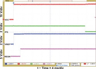
- 7.3.16 PG Output
- 7.3.17 CE (Charge Enable)
- 7.3.18 Inductor, Capacitor, and Sense Resistor Selection Guidelines
- 7.3.19 Charge Status Outputs
- 7.3.20 Battery Detection
- 7.4 Device Functional Modes
- 7.5 Application Information
- 7.6 Typical Application
- 8 Power Supply Recommendations
- 9 Layout
- 10Device and Documentation Support
- 11Mechanical, Packaging, and Orderable Information
6 Specifications
6.1 Absolute Maximum Ratings(1)(2)(3)
over operating free-air temperature range (unless otherwise noted)| MIN | MAX | UNIT | ||
|---|---|---|---|---|
| Voltage range | VCC, SRP, SRN, CE, STAT, PG | –0.3 | 33 | V |
| PH | –2 | 36 | V | |
| VFB | –0.3 | 16 | V | |
| REGN, LODRV, TS | –0.3 | 7 | V | |
| BTST, HIDRV with respect to GND | –0.3 | 39 | V | |
| VREF, ISET | –0.3 | 3.6 | V | |
| Maximum difference voltage | SRP–SRN | –0.5 | 0.5 | V |
| Junction temperature range, TJ | –40 | 155 | ºC | |
(1) Stresses beyond those listed under Absolute Maximum Ratings may cause permanent damage to the device. These are stress ratings only, and functional operation of the device at these or any other conditions beyond those indicated under Recommended Operating Conditions is not implied. Exposure to absolute-maximum-rated conditions for extended periods may affect device reliability.
(2) All voltages are with respect to GND if not specified. Currents are positive into, negative out of the specified terminal. Consult Packaging Section of the data book for thermal limitations and considerations of packages.
(3) Must have a series resistor between battery pack and VFB if battery-pack voltage is expected to be greater than 16 V. Usually the resistor-divider top resistor takes care of this.
6.2 Handling Ratings
| MIN | MAX | UNIT | |||
|---|---|---|---|---|---|
| Tstg | Storage temperature range | –55 | 155 | °C | |
| V(ESD) | Electrostatic discharge | Human body model (HBM), per ANSI/ESDA/JEDEC JS-001, all pins(1) | –1000 | 1000 | V |
| Charged device model (CDM), per JEDEC specification JESD22-C101, all pins(2) | –250 | 250 | |||
(1) JEDEC document JEP155 states that 500-V HBM allows safe manufacturing with a standard ESD control process.
(2) JEDEC document JEP157 states that 250-V CDM allows safe manufacturing with a standard ESD control process.
6.3 Recommended Operating Conditions
| VALUE | UNIT | ||
|---|---|---|---|
| Voltage range | VCC, SRP, SRN, CE, STAT, PG | –0.3 to 28 | V |
| PH | –2 to 30 | V | |
| VFB | –0.3 to 14 | V | |
| REGN, LODRV, TS | –0.3 to 6.5 | V | |
| BTST, HIDRV with respect to GND | –0.3 to 34 | V | |
| ISET | –0.3 to 3.3 | V | |
| VREF | 3.3 | V | |
| Maximum difference voltage | SRP–SRN | –0.2 to 0.2 | V |
| Junction temperature range, TJ | 0 to 125 | ºC | |
6.4 Thermal Information
| THERMAL METRIC(1) | RVA | UNIT | |
|---|---|---|---|
| 16 PINS | |||
| RθJA | Junction-to-ambient thermal resistance | 43.8 | °C/W |
| RθJC(top) | Junction-to-case (top) thermal resistance | 81 | |
| RθJB | Junction-to-board thermal resistance | 16 | |
| ψJT | Junction-to-top characterization parameter | 0.6 | |
| ψJB | Junction-to-board characterization parameter | 15.77 | |
| RθJC(bot) | Junction-to-case (bottom) thermal resistance | 4 | |
(1) For more information about traditional and new thermal metrics, see the IC Package Thermal Metrics application report, SPRA953.
6.5 Electrical Characteristics
5 V ≤ VVCC ≤ 28 V, 0°C < TJ < 125°C, typical values are at TA = 25°C, with respect to GND (unless otherwise noted)| PARAMETER | TEST CONDITIONS | MIN | TYP | MAX | UNIT | |
|---|---|---|---|---|---|---|
| OPERATING CONDITIONS | ||||||
| VVCC_OP | VCC input voltage operating range | 5 | 28 | V | ||
| QUIESCENT CURRENTS | ||||||
| IBAT | Total battery discharge current (sum of currents into VCC, BTST, PH, SRP, SRN, VFB), VFB ≤ 2.1 V | VVCC < VSRN, VVCC > VUVLO (SLEEP) | 15 | μA | ||
| IAC | Adapter supply current (current into VCC pin) |
VVCC > VSRN, VVCC > VUVLO CE = LOW (IC quiescent current) | 1 | 1.5 | mA | |
| VVCC > VSRN, VVCC >VVCCLOW, CE = HIGH, charge done | 2 | 5 | ||||
| VVCC > VSRN, VVCC >VVCCLOW, CE = HIGH, Charging, Qg_total = 20 nC, VVCC= 20 V | 50 | |||||
| CHARGE VOLTAGE REGULATION | ||||||
| VFB | Feedback regulation voltage | 2.1 | V | |||
| Charge voltage regulation accuracy | TJ = 0°C to 85°C | –0.5% | 0.5% | |||
| TJ = –40°C to 125°C | –0.7% | 0.7% | ||||
| IVFB | Leakage Current into VFB pin | VFB = 2.1 V | 100 | nA | ||
| CURRENT REGULATION – FAST CHARGE | ||||||
| VISET | ISET voltage range | 2 | V | |||
| VIREG_CHG | SRP-SRN current sense voltage range | VIREG_CHG = VSRP – VSRN | 100 | mV | ||
| KISET | Charge current set factor (amps of charge current per volt on ISET pin) | RSENSE = 10 mΩ | 5 | A/V | ||
| Charge current regulation accuracy | VIREG_CHG = 40 mV | –3% | 3% | |||
| VIREG_CHG = 20 mV | –4% | 4% | ||||
| VIREG_CHG = 5 mV | –25% | 25% | ||||
| VIREG_CHG = 1.5 mV (VSRN > 3.1 V) | –40% | 40% | ||||
| IISET | Leakage current into ISET pin | VISET = 2 V | 100 | nA | ||
| CURRENT REGULATION – PRECHARGE | ||||||
| Precharge current range | RSENSE = 10 mΩ | ICHARGE/10 | A | |||
| KPRECH | Precharge current set factor (amps of precharge current per volt on ISET pin) | RSENSE = 10 mΩ | 0.5 | A/V | ||
| Precharge current regulation accuracy | VIREG_PRECH = 10 mV | –10% | 10% | |||
| VIREG_PRECH = 5 mV | –25% | 25% | ||||
| VIREG_PRECH = 1.5 mV (VSRN < 3.1 V) | –55% | 55% | ||||
| CHARGE TERMINATION | ||||||
| Termination current range | RSENSE = 10 mΩ | ICHARGE/10 | A | |||
| KTERM | Termination current set factor (amps of termination current per volt on ISET pin) | RSENSE = 10 mΩ | 0.5 | A/V | ||
| Termination current accuracy | VITERM = 10 mV | –10% | 10% | |||
| VITERM = 5 mV | –25% | 25% | ||||
| VITERM = 1.5 mV | –45% | 45% | ||||
| IQUAL | Termination qualification current | Discharge current once termination is detected | 2 | mA | ||
| INPUT UNDERVOLTAGE LOCKOUT COMPARATOR (UVLO) | ||||||
| VUVLO | AC undervoltage rising threshold | Measure on VCC | 3.65 | 3.85 | 4 | V |
| VUVLO_HYS | AC undervoltage hysteresis, falling | 350 | mV | |||
| VCC LOWV COMPARATOR | ||||||
| Falling threshold, disable charge | Measure on VCC | 4.1 | V | |||
| Rising threshold, resume charge | 4.35 | 4.5 | V | |||
| SLEEP COMPARATOR (REVERSE DISCHARGING PROTECTION) | ||||||
| VSLEEP _FALL | SLEEP falling threshold | VVCC – VSRN to enter SLEEP | 40 | 100 | 150 | mV |
| VSLEEP_HYS | SLEEP hysteresis | 500 | mV | |||
| BAT LOWV COMPARATOR | ||||||
| VLOWV | Precharge to fast-charge transition (LOWV threshold) | Measured on VFB pin | 1.534 | 1.55 | 1.566 | V |
| VLOWV_HYS | LOWV hysteresis | 100 | mV | |||
| RECHARGE COMPARATOR | ||||||
| VRECHG | Recharge threshold (with respect to.VREG) | Measured on VFB pin | 35 | 50 | 65 | mV |
| BAT OVER-VOLTAGE COMPARATOR | ||||||
| VOV_RISE | Overvoltage rising threshold | As percentage of VFB | 104% | |||
| VOV_FALL | Overvoltage falling threshold | As percentage of VFB | 102% | |||
| INPUT OVER-VOLTAGE COMPARATOR (ACOV) | ||||||
| VACOV | AC overvoltage rising threshold on VCC | 31.04 | 32 | 32.96 | V | |
| VACOV_HYS | AC overvoltage falling hysteresis | 1 | V | |||
| THERMAL SHUTDOWN COMPARATOR | ||||||
| TSHUT | Thermal shutdown rising temperature | Temperature increasing | 145 | °C | ||
| TSHUT_HYS | Thermal shutdown hysteresis | 15 | °C | |||
| THERMISTOR COMPARATOR | ||||||
| VLTF | Cold temperature rising threshold | As percentage to VVREF | 72.5% | 73.5% | 74.5% | |
| VLTF_HYS | Rising hysteresis | As percentage to VVREF | 0.2% | 0.4% | 0.6% | |
| VHTF | Hot temperature rising threshold | As percentage to VVREF | 36.2% | 37% | 37.8% | |
| VTCO | Cutoff temperature rising threshold | As percentage to VVREF | 33.7% | 34.4% | 35.1% | |
| Deglitch time for temperature out of range detection | VTS > VLTF, or VTS < VTCO, or VTS < VHTF | 400 | ms | |||
| Deglitch time for temperature in valid range detection | VTS < VLTF – VLTF_HYS or VTS >VTCO, or VTS > VHTF | 20 | ms | |||
| CHARGE OVERCURRENT COMPARATOR (CYCLE-BY-CYCLE) | ||||||
| VOC | Charge overcurrent falling threshold | Current rising, in non-synchronous mode, mesure on V(SRP-SRN), VSRP < 2 V | 45.5 | mV | ||
| Current rising, as percentage of V(IREG_CHG), in synchronous mode, VSRP > 2.2 V | 160% | |||||
| Charge overcurrent threshold floor | Minimum OCP threshold in synchronous mode, measure on V(SRP-SRN), VSRP > 2.2 V | 50 | mV | |||
| Charge over-current threshold ceiling | Maximum OCP threshold in synchronous mode, measure on V(SRP-SRN), VSRP > 2.2 V | 180 | mV | |||
| CHARGE UNDERCURRENT COMPARATOR (CYCLE-BY-CYCLE) | ||||||
| VISYNSET | Charge under-current falling threshold | VSRP>2.2 V, switch from CCM to DCM | 1 | 5 | 9 | mV |
| BATTERY SHORTED COMPARATOR (BATSHORT) | ||||||
| VBATSHT | BAT Short falling threshold, forced non-syn mode | VSRP falling | 2 | V | ||
| VBATSHT_HYS | BAT short rising hysteresis | 200 | mV | |||
| LOW CHARGE CURRENT COMPARATOR | ||||||
| VLC | Low charge current (average) falling threshold to force into non-sync mode | Measure V(SRP-SRN) | 1.25 | mV | ||
| VLC_HYS | Low charge current rising hysteresis | 1.25 | mV | |||
| VREF REGULATOR | ||||||
| VVREF_REG | VREF regulator voltage | VVCC > VUVLO (0 - 35-mA load) | 3.267 | 3.3 | 3.333 | V |
| IVREF_LIM | VREF current limit | VVREF = 0 V, VVCC > VUVLO | 35 | mA | ||
| REGN REGULATOR | ||||||
| VREGN_REG | REGN regulator voltage | VVCC > 10 V, CE = HIGH (0 - 40 mA load) | 5.7 | 6.0 | 6.3 | V |
| IREGN_LIM | REGN current limit | VREGN = 0 V, VVCC > VUVLO | 40 | mA | ||
| BATTERY DETECTION | ||||||
| IWAKE | Wake current | RSENSE = 10 mΩ | 50 | 125 | 200 | mA |
| IDISCHARGE | Discharge current | 8 | mA | |||
| IFAULT | Fault current after a timeout fault | 2 | mA | |||
| VWAKE | Wake threshold (relative to VREG) | Voltage on VFB to detect battery absent during wake | 50 | mV | ||
| VDISCH | Discharge threshold | Voltage on VFB to detect battery absent during discharge | 1.55 | V | ||
| PWM HIGH SIDE DRIVER (HIDRV) | ||||||
| RDS_HI_ON | High-side driver (HSD) turnon resistance | VBTST – VPH = 5.5 V | 3.3 | 6 | Ω | |
| RDS_HI_OFF | High-side driver turnoff resistance | VBTST – VPH = 5.5 V | 1 | 1.3 | Ω | |
| VBTST_REFRESH | Bootstrap refresh comparator threshold voltage | VBTST – VPH when low side refresh pulse is requested | 4 | 4.2 | V | |
| PWM LOW SIDE DRIVER (LODRV) | ||||||
| RDS_LO_ON | Low-side driver (LSD) turnon resistance | 4.1 | 7 | Ω | ||
| RDS_LO_OFF | Low-side driver turnoff resistance | 1 | 1.4 | Ω | ||
| PWM OSCILLATOR | ||||||
| VRAMP_HEIGHT | PWM ramp height | As percentage of VCC | 7% | |||
| PWM switching frequency(1) | 1020 | 1200 | 1380 | kHz | ||
| INTERNAL SOFT START (8 steps to regulation current ICHARGE) | ||||||
| Soft-start steps | 8 | step | ||||
| CHARGER SECTION POWER-UP SEQUENCING | ||||||
| Charge-enable delay after power up | Delay from when CE = 1 to when the charger is allowed to turn on | 1.5 | s | |||
| LOGIC IO PIN CHARACTERISTICS (CE, STAT, PG) | ||||||
| VIN_LO | CE input low threshold voltage | 0.8 | V | |||
| VIN_HI | CE input high threshold voltage | 2.1 | ||||
| VBIAS_CE | CE input bias current | V = 3.3 V (CE has internal 1MΩ pulldown resistor) | 6 | μA | ||
| VOUT_LO | STAT, PG output low saturation voltage | Sink current = 5 mA | 0.5 | V | ||
| IOUT_HI | Leakage current | V = 32 V | 1.2 | µA | ||
(1) Specified by design.
6.6 Timing Requirements
| MIN | TYP | MAX | UNIT | |||
|---|---|---|---|---|---|---|
| CHARGE TERMINATION | ||||||
| Deglitch time for termination (both edges) | 100 | ms | ||||
| tQUAL | Termination qualification time | VBAT > VRECH and ICHARGE < ITERM | 250 | ms | ||
| SLEEP COMPARATOR (REVERSE DISCHARGING PROTECTION) | ||||||
| SLEEP rising delay | VCC falling below SRN, delay to pull up PG | 1 | µs | |||
| SLEEP falling delay | VCC rising above SRN, delay to pull down PG | 30 | ms | |||
| SLEEP rising shutdown deglitch | VCC falling below SRN, delay to enter SLEEP mode | 100 | ms | |||
| SLEEP falling powerup deglitch | VCC rising above SRN, delay to come out of SLEEP mode | 30 | ms | |||
| BAT LOWV COMPARATOR | ||||||
| LOWV rising deglitch | VFB falling below VLOWV | 25 | ms | |||
| LOWV falling deglitch | VFB rising above VLOWV + VLOWV_HYS | 25 | ms | |||
| RECHARGE COMPARATOR | ||||||
| Recharge rising deglitch | VFB decreasing below VRECHG | 10 | ms | |||
| Recharge falling deglitch | VFB increasing above VRECHG | 10 | ms | |||
| INPUT OVER-VOLTAGE COMPARATOR (ACOV) | ||||||
| VACOV_HYS | AC overvoltage rising deglitch | 1 | ms | |||
| AC overvoltage falling deglitch | 1 | ms | ||||
| THERMISTOR COMPARATOR | ||||||
| Thermal shutdown rising deglitch | Temperature increasing | 100 | μs | |||
| Thermal shutdown falling deglitch | Temperature decreasing | 10 | ms | |||
| BATTERY SHORTED COMPARATOR (BATSHORT) | ||||||
| VBATSHT_DEG | Deglitch on both edges | 1 | μs | |||
| LOW CHARGE CURRENT COMPARATOR | ||||||
| VLC_DEG | Deglitch on both edges | 1 | μs | |||
| SAFETY TIMER | ||||||
| tPRECHG | Precharge safety timer range(1) | Precharge time before fault occurs | 1440 | 1800 | 2160 | s |
| tCHARGE | Internal five hour safety timer(1) | 4.25 | 5 | 5.75 | hr | |
| BATTERY DETECTION | ||||||
| tWAKE | Wake timer | Max time charge is enabled | 500 | ms | ||
| tDISCHARGE | Discharge timer | Max time discharge current is applied | 1 | s | ||
| PWM DRIVERS TIMING | ||||||
| Driver dead time | Dead time when switching between LSD and HSD, no load at LSD and HSD | 30 | ns | |||
| INTERNAL SOFT START (8 steps to regulation current ICHARGE) | ||||||
| Soft-start step time | 1.6 | ms | ||||