SLUS891B February 2010 – November 2014
PRODUCTION DATA.
- 1 Features
- 2 Applications
- 3 Description
- 4 Revision History
- 5 Pin Configuration and Functions
- 6 Specifications
-
7 Detailed Description
- 7.1 Overview
- 7.2 Functional Block Diagram
- 7.3
Feature Description
- 7.3.1 Battery Voltage Regulation
- 7.3.2 Battery Current Regulation
- 7.3.3 Precharge
- 7.3.4 Charge Termination, Recharge, and Safety Timer
- 7.3.5 Power Up
- 7.3.6 Enable and Disable Charging
- 7.3.7 Automatic Internal Soft-Start Charger Current
- 7.3.8 Cycle-by-Cycle Charge Undercurrent Protection
- 7.3.9 Input Overvoltage Protection (ACOV)
- 7.3.10 Input Undervoltage Lock-Out (UVLO)
- 7.3.11 Battery Overvoltage Protection
- 7.3.12 Cycle-by-Cycle Charge Overcurrent Protection
- 7.3.13 Thermal Shutdown Protection
- 7.3.14 Temperature Qualification
- 7.3.15 Timer Fault Recovery
- 7.3.16 PG Output
- 7.3.17 CE (Charge Enable)
- 7.3.18 Inductor, Capacitor, and Sense Resistor Selection Guidelines
- 7.3.19 Charge Status Outputs
- 7.3.20 Battery Detection
- 7.4 Device Functional Modes
- 7.5 Application Information
- 7.6 Typical Application
- 8 Power Supply Recommendations
- 9 Layout
- 10Device and Documentation Support
- 11Mechanical, Packaging, and Orderable Information
9 Layout
9.1 Layout Guidelines
The switching node rise and fall times should be minimized for minimum switching loss. Proper layout of the components to minimize high-frequency current-path loop (see Figure 19) is important to prevent electrical and magnetic field radiation and high-frequency resonant problems. Here is a PCB priority list for proper layout. Layout of the PCB according to this specific order is essential.
- Place the input capacitor as close as possible to switching the MOSFET supply and ground connections, and use the shortest possibloe copper trace connection. These parts should be placed on the same layer of PCB instead of on different layers, using vias to make this connection.
- The IC should be placed close to the switching MOSFET gate terminals to keep the gate-drive signal traces short for a clean MOSFET drive. The IC can be placed on the other side of the PCB from the switching MOSFET.
- Place the inductor input terminal as close as possible to the switching MOSFET output terminal. Minimize the copper area of this trace to lower electrical and magnetic field radiation but make the trace wide enough to carry the charging current. Do not use multiple layers in parallel for this connection. Minimize parasitic capacitance from this area to any other trace or plane.
- The charging-current sensing resistor should be placed right next to the inductor output. Route the sense leads connected across the sensing resistor back to the IC in same layer, close to each other (minimize loop area) and do not route the sense leads through a high-current path (see Figure 18 for Kelvin connection for best current accuracy). Place the decoupling capacitor on these traces next to the IC.
- Place the output capacitor next to the sensing resistor output and ground.
- Output capacitor ground connections must be tied to the same copper that connects to the input capacitor ground before connecting to system ground.
- Route the analog ground separately from the power ground and use a single ground connection to tie the charger power ground to the charger analog ground. Just beneath the IC, use copper pour for analog ground, but avoid the power pins to reduce inductive and capacitive noise coupling. Connect the analog ground to GND. Connect the analog ground and power ground together using the thermal pad as the single ground connection point. Or use a 0-Ω resistor to tie the analog ground to power ground (the thermal pad should tie to analog ground in this case). A star connection under the thermal pad is highly recommended.
- It is critical that the exposed thermal pad on the back side of the IC package be soldered to the PCB ground. Ensure that there are sufficient thermal vias directly under the IC connecting to the ground plane on the other layers.
- Place decoupling capacitors next to the IC pins, and make trace connections as short as possible.
- All via sizes and numbers should be enough for a given current path.
See the EVM design (SLUU410) for the recommended component placement with trace and via locations.
9.2 Layout Example
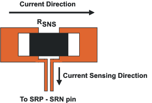 Figure 18. Sensing Resistor PCB Layout
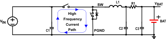 Figure 19. High Frequency Current Path