SLUS891B February 2010 – November 2014
PRODUCTION DATA.
- 1 Features
- 2 Applications
- 3 Description
- 4 Revision History
- 5 Pin Configuration and Functions
- 6 Specifications
-
7 Detailed Description
- 7.1 Overview
- 7.2 Functional Block Diagram
- 7.3
Feature Description
- 7.3.1 Battery Voltage Regulation
- 7.3.2 Battery Current Regulation
- 7.3.3 Precharge
- 7.3.4 Charge Termination, Recharge, and Safety Timer
- 7.3.5 Power Up
- 7.3.6 Enable and Disable Charging
- 7.3.7 Automatic Internal Soft-Start Charger Current
- 7.3.8 Cycle-by-Cycle Charge Undercurrent Protection
- 7.3.9 Input Overvoltage Protection (ACOV)
- 7.3.10 Input Undervoltage Lock-Out (UVLO)
- 7.3.11 Battery Overvoltage Protection
- 7.3.12 Cycle-by-Cycle Charge Overcurrent Protection
- 7.3.13 Thermal Shutdown Protection
- 7.3.14 Temperature Qualification
- 7.3.15 Timer Fault Recovery
- 7.3.16 PG Output
- 7.3.17 CE (Charge Enable)
- 7.3.18 Inductor, Capacitor, and Sense Resistor Selection Guidelines
- 7.3.19 Charge Status Outputs
- 7.3.20 Battery Detection
- 7.4 Device Functional Modes
- 7.5 Application Information
- 7.6 Typical Application
- 8 Power Supply Recommendations
- 9 Layout
- 10Device and Documentation Support
- 11Mechanical, Packaging, and Orderable Information
Application and Implementation
NOTE
Information in the following applications sections is not part of the TI component specification, and TI does not warrant its accuracy or completeness. TI’s customers are responsible for determining suitability of components for their purposes. Customers should validate and test their design implementation to confirm system functionality.
7.5 Application Information
The evaluation module (EVM) is a complete charger module for evaluating a stand-alone single multi-cell Li-ion charger using the bq241600 device.
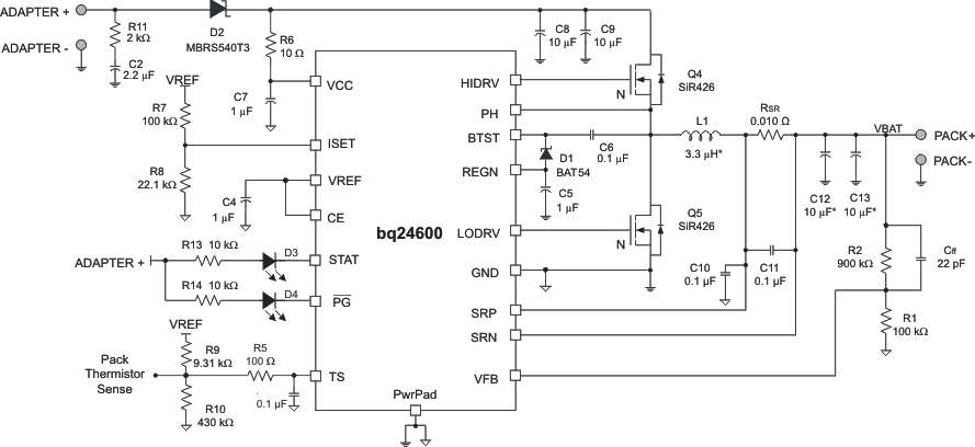
7.6 Typical Application
The typical application shown is a 28-V input, 5-cell Li-ion, 3-A charger.
7.6.1 Design Requirements
For this design example, use the parameters shown in Table 3.
Table 3. Design Parameters
| PARAMETER | VALUE |
|---|---|
| Input voltage | 28 V |
| Battery Charge Voltage | 21 V |
| Battery Charge Current | 3 A |
Table 4. Supporting Components for Figure 11
7.6.2 Detailed Design Procedure
7.6.2.1 Inductor Selection
The bq24600 has a 1.2-MHz switching frequency to allow the use of small inductor and capacitor values. Inductor saturation current should be higher than the charging current (ICHARGE) plus half the ripple current (IRIPPLE):

The inductor ripple current depends on input voltage (VIN), duty cycle (D = VOUT/VIN), switching frequency (fs) and inductance (L):
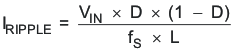
The maximum inductor ripple current happens with D = 0.5 or close to 0.5. For example, the battery charging voltage range is from 9 V to 12.6 V for a 3-cell battery pack. For a 20-V adapter voltage, 10-V battery voltage gives the maximum inductor ripple current. Another example is a 4-cell battery, for which the battery voltage range is from 12 V to 16.8 V, and 12-V battery voltage gives the maximum inductor ripple current.
Usually, inductor ripple is designed in the range of 20%–40% of maximum charging current as a trade-off between inductor size and efficiency for a practical design.
The bq24600 has cycle-by-cycle charge undercurrent protection (UCP) by monitoring the charging-current-sensing resistor to prevent negative inductor current. The typical UCP threshold is 5 mV falling edge, corresponding to 0.5-A falling edge for a 10-mΩ charging-current-sensing resistor.
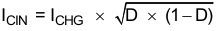
7.6.2.2 Input Capacitor
The input capacitor should have enough ripple-current rating to absorb the input switching-ripple current. The worst-case rms ripple current is half of the charging current when the duty cycle is 0.5. If the converter does not operate at 50% duty cycle, then the worst-case capacitor rms current ICIN occurs where the duty cycle is closest to 50% and can be estimated by the following equation:
7.6.2.3 Output Capacitor
A low-ESR ceramic capacitor such as X7R or X5R is preferred for the input decoupling capacitor and should be placed near the drain of the high-side MOSFET and the source of the low-side MOSFET as close as possible. The voltage rating of the capacitor must be higher than the normal input voltage level. A 25-V rating or higher capacitor is preferred for a 20-V input voltage. A 10-µF to 20-µF capacitance is suggested for typical of 3-A to 4-A charging current.
The output capacitor also should have enough ripple-current rating to absorb the output switching ripple current. The output capacitor rms current ICOUT is given:

The output capacitor voltage ripple can be calculated as follows:
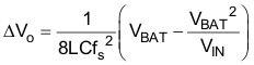
At certain input/output voltage and switching frequency, the voltage ripple can be reduced by increasing the output filter LC.
The bq24600 has an internal loop compensator. To get good loop stability, the resonant frequency of the output inductor and output capacitor should be designed between 17 kHz and 25 kHz. The preferred ceramic capacitor for a 4-cell application has a 25-V or higher rating and X7R or X5R dielectric.
7.6.2.4 Power MOSFET Selection
Two external N-channel MOSFETs are used for a synchronous switching battery charger. The gate drivers are internally integrated into the IC with 6 V of gate drive voltage. 30-V or higher voltage rating MOSFETs are preferred for 20-V input voltage, and 40-V or higher rating MOSFETs are preferred for 20-V to 28-V input voltage.
Figure-of-merit (FOM) is usually used for selecting the proper MOSFET based on a tradeoff between the conduction loss and switching loss. For a top-side MOSFET, FOM is defined as the product of a MOSFET on-resistance, rDS(on), and the gate-to-drain charge, QGD. For a bottom-side MOSFET, FOM is defined as the product of the MOSFET on-resistance, rDS(on), and the total gate charge, QG.

The lower the FOM value, the lower the total power loss. Usually lower rDS(on) has higher cost with the same package size.
The top-side MOSFET loss includes conduction loss and switching loss. It is a function of duty cycle (D = VOUT/VIN), charging current (ICHARGE), the MOSFET on-resistance rDS(on)), input voltage (VIN), switching frequency (fS), turnon time (ton) and turnoff time (ttoff):

The first item represents the conduction loss. Usually, MOSFET rDS(on) increases by 50% with a 100ºC junction-temperature rise. The second term represents the switching loss. The MOSFET turnon and turnoff times are given by:
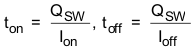
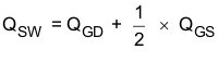
where Qsw is the switching charge, Ion is the turnon gate-drive current and Ioff is the turnoff gate-drive current. If the switching charge is not given in the MOSFET data sheet, it can be estimated by gate-to-drain charge (QGD) and gate-to-source charge (QGS):
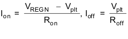
Total gate-drive current can be estimated by REGN voltage (VREGN), MOSFET plateau voltage (Vplt), total turn-on gate resistance (Ron) and turn-off gate resistance Roff) of the gate driver:
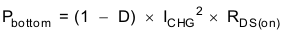
The conduction loss of the bottom-side MOSFET is calculated with the following equation when it operates in synchronous continuous-conduction mode:
If the SRP-SRN voltage decreases below 5 mV (the charger is also forced into non-synchronous mode when the average SRP-SRN voltage is lower than 1.25 mV), the low side FET is turned off for the remainder of the switching cycle to prevent negative inductor current.
As a result, all the freewheeling current goes through the body diode of the bottom-side MOSFET. The maximum charging current in non-synchronous mode can be up to 0.9 A (0.5 A typ.) for a 10-mΩ charging-current sensing resistor considering IC tolerance. Choose the bottom-side MOSFET with either an internal Schottky or body diode capable of carrying the maximum non-synchronous-mode charging current.
MOSFET gate driver power loss contributes to the dominant losses on the controller IC when the buck converter is switching. Choosing a MOSFET with a small Qg_total largely reduces the IC power loss to avoid thermal shutdown.

where Qg_total is the total gate charge for both upper and lower MOSFETs at 6-V VREGN.
7.6.2.5 Input Filter Design
During adapter hot plug-in, the parasitic inductance and input capacitor from the adapter cable form a second-order system. The voltage spike at the VCC pin may be beyond the IC maximum voltage rating and damage IC. The input filter must be carefully designed and tested to prevent an overvoltage event on the VCC pin.
There are several methods for damping or limiting the overvoltage spike during adapter hot plug-in. An electrolytic capacitor with high ESR as an input capacitor can damp the overvoltage spike well below the IC maximum pin voltage rating. A high-current-capability TVS Zener diode can also limit the overvoltage level to an IC-safe level. However these two solutions may not have low cost or small size.
A cost-effective and small-size solution is shown in Figure 12. R1 and C1 comprise a damping RC network to damp the hot plug-in oscillation. As a result, the overvoltage spike is limited to a safe level. D1 is used for reverse voltage protection for the VCC pin (it can be the input Schottky diode or the body diode of input ACFET). C2 is the VCC pin decoupling capacitor and it should be placed as close as possible to the VCC pin. R2 and C2 form a damping RC network to further protect the IC from high dv/dt and high-voltage spikes. The C2 value should be less than the C1 value so R1 can be dominant over the ESR of C1 to get enough damping effect for hot plug-in. The R1 and R2 packages must be sized to handle inrush-current power loss according to resistor manufacturer’s datasheet. The filter component values must always be verified with the real application and minor adjustments may be needed to fit in the real application circuit.
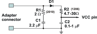 Figure 12. Input Filter
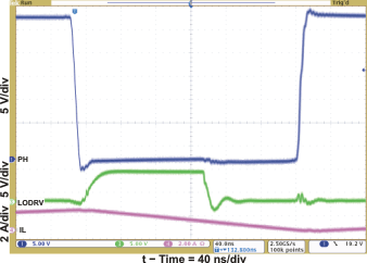
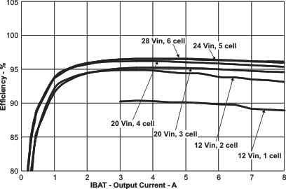
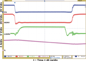
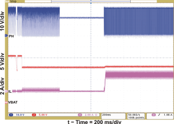
7.6.3 Application Curves
| CE = 1 |