SLUSA76B December   2010  – January 2015

PRODUCTION DATA.  

  1. Features
  2. Applications
  3. Description
  4. Typical Application Schematic
  5. Revision History
  6. Pin Configuration and Functions
  7. Specifications
    1. 7.1 Absolute Maximum Ratings
    2. 7.2 ESD Ratings
    3. 7.3 Recommended Operating Conditions
    4. 7.4 Thermal Information
    5. 7.5 Electrical Characteristics
    6. 7.6 Typical Characteristics
  8. Detailed Description
    1. 8.1 Overview
    2. 8.2 Functional Block Diagram
    3. 8.3 Feature Description
      1. 8.3.1 Input Voltage-Based Dynamic Power Management (VBUS-DPM)
      2. 8.3.2 CHG Pin Indication
      3. 8.3.3 CHG and PG LED Pull-Up Source
      4. 8.3.4 Power Good Indication (PG)
    4. 8.4 Device Functional Modes
      1. 8.4.1 Power-Down or Undervoltage Lockout (UVLO)
      2. 8.4.2 Operation Mode Detection and Transition
      3. 8.4.3 Sleep Mode
      4. 8.4.4 Load Mode
      5. 8.4.5 Charge Mode
        1. 8.4.5.1  Overvoltage Protection (OVP) - Continuously Monitored
        2. 8.4.5.2  Power Up
        3. 8.4.5.3  Battery Detect Routine
        4. 8.4.5.4  New Charge Cycle
        5. 8.4.5.5  BAT Output
        6. 8.4.5.6  Fast Charge Current (IOUT)
        7. 8.4.5.7  Termination
        8. 8.4.5.8  Timers
        9. 8.4.5.9  Battery Temperature Monitoring
        10. 8.4.5.10 Limited Power Charge Mode - TS Pin High
      6. 8.4.6 Suspend Mode
  9. Application and Implementation
    1. 9.1 Application Information
    2. 9.2 Typical Application
      1. 9.2.1 Design Requirements
      2. 9.2.2 Detailed Design Procedure
      3. 9.2.3 Application Curves
  10. 10Power Supply Recommendations
  11. 11Layout
    1. 11.1 Layout Guidelines
    2. 11.2 Layout Example
  12. 12Device and Documentation Support
    1. 12.1 Device Support
      1. 12.1.1 Third-Party Products Disclaimer
    2. 12.2 Trademarks
    3. 12.3 Electrostatic Discharge Caution
    4. 12.4 Glossary
  13. 13Mechanical, Packaging, and Orderable Information

封装选项

机械数据 (封装 | 引脚)
散热焊盘机械数据 (封装 | 引脚)
订购信息

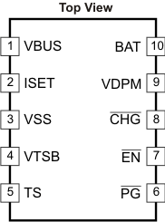
6 Pin Configuration and Functions

DQC Package
10 Pins
po_lusa76.gif

Pin Functions

PIN I/O DESCRIPTION
NAME NO.
BAT 10 I/O Battery Connection. System Load may be connected.
Expected range of bypass capacitors 1 μF to 10 μF, connected from BAT to VSS.
CHG 8 O Charge Status indication, Low (FET ON) indicates charging, and High impedance (open drain FET OFF) in other cases
EN 7 I Chip enable control. Low to enable charge or load mode, and high to enable suspend mode.
ISET 2 I Programs the Fast-charge current setting. External resistor from ISET to VSS defines fast charge current value.
PG 6 O Power Present indication. LOW (FET ON) When input voltage is in normal range (VBUS>BAT and VBUS>UVLO), High impedance (open drain FET OFF) in other cases.
TS 5 I Temperature sense pin, connected to NTC Thermistor in the battery pack. Pulling High puts part in limited power charging mode. Must not be left floating.
VBUS 1 I/O For charging mode, input for charging source, connect to external DC supply (ie, Solar Panel, Inductive charging PAD, or Wall Adapter) For load mode, output for current limited battery voltage.
Expected range of bypass capacitors 1 μF to 10 μF, connected from VBUS to VSS.
VDPM 9 I Programs the input voltage regulation threshold.
Expected range of programming resistor is 1 kΩ to 10 kΩ, connected from VDPM to VSS. When VDPM is floating, the VIN DPM loop operates in battery tracking mode, and the VIN DPM threshold is BAT+100 mV (BAT>3.6 V) or 3.7 V (BAT≤3.6 V) in this case. VIN DPM threshold should be programmed higher than battery voltage to ensure proper operation.
VSS 3 Ground terminal
VTSB 4 O TS bias reference voltage pin, regulated output. No external capacitor is required from VTSB to VSS. Only enabled during charge.
Thermal PAD and Package There is an internal electrical connection between the exposed thermal pad and the VSS pin of the device. The thermal pad must be connected to the same potential as the VSS pin on the printed circuit board. Do not use the thermal pad as the primary ground input for the device. VSS pin must be connected to ground at all times.