SLUSA76B December 2010 – January 2015
PRODUCTION DATA.
- 1 Features
- 2 Applications
- 3 Description
- 4 Typical Application Schematic
- 5 Revision History
- 6 Pin Configuration and Functions
- 7 Specifications
-
8 Detailed Description
- 8.1 Overview
- 8.2 Functional Block Diagram
- 8.3 Feature Description
- 8.4
Device Functional Modes
- 8.4.1 Power-Down or Undervoltage Lockout (UVLO)
- 8.4.2 Operation Mode Detection and Transition
- 8.4.3 Sleep Mode
- 8.4.4 Load Mode
- 8.4.5
Charge Mode
- 8.4.5.1 Overvoltage Protection (OVP) - Continuously Monitored
- 8.4.5.2 Power Up
- 8.4.5.3 Battery Detect Routine
- 8.4.5.4 New Charge Cycle
- 8.4.5.5 BAT Output
- 8.4.5.6 Fast Charge Current (IOUT)
- 8.4.5.7 Termination
- 8.4.5.8 Timers
- 8.4.5.9 Battery Temperature Monitoring
- 8.4.5.10 Limited Power Charge Mode - TS Pin High
- 8.4.6 Suspend Mode
- 9 Application and Implementation
- 10Power Supply Recommendations
- 11Layout
- 12Device and Documentation Support
- 13Mechanical, Packaging, and Orderable Information
8 Detailed Description
8.1 Overview
The bq24210 is a highly integrated 2-mm x 3-mm2 single-cell Li-Ion charger with bidirectional power flow capability. Depending on the status of control pins and source conditions, the IC can operate in several modes: sleep, charge, load, and suspend mode.
At power up (VBUS or BAT ramps up, or EN pin changes status), the IC performs the operation mode detection automatically. Depending on the VBUS and BAT levels, the IC enters sleep, charge, load, or suspend mode.
In charge mode, the charger has three phases of charging: Pre-charge to recondition a full discharged battery, fast-charge constant current to supply the buck charge safely and voltage regulation to safely reach full capacity, as shown in Figure 3. The charge operating mode is very flexible, allowing programming of the fast-charge current, and input voltage regulation threshold. The programmable input voltage regulation threshold makes the IC compatible with both low impedane power sources, like USB ports or wall adapters, or high impedance sources such as solar panel or thermo-electric generators.
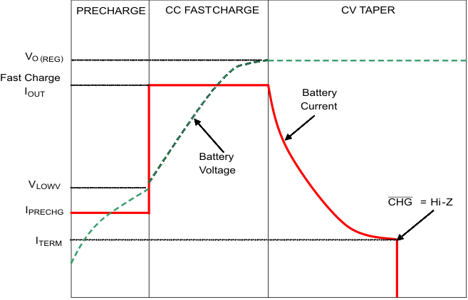 Figure 3. Charge Profile
In load mode, the IC connects the battery voltage to the input pin (VBUS pin) through the back to back FET (Q1 and Q2) to power the load connected at VBUS pin. The load current is limited to provide overload protection.
In sleep mode, Q2 is OFF and the IC standby current is reduced to ICC_REV.
In suspend mode, the IC turns off both Q1 and Q2, and no charging or reverse conduction is allowed.
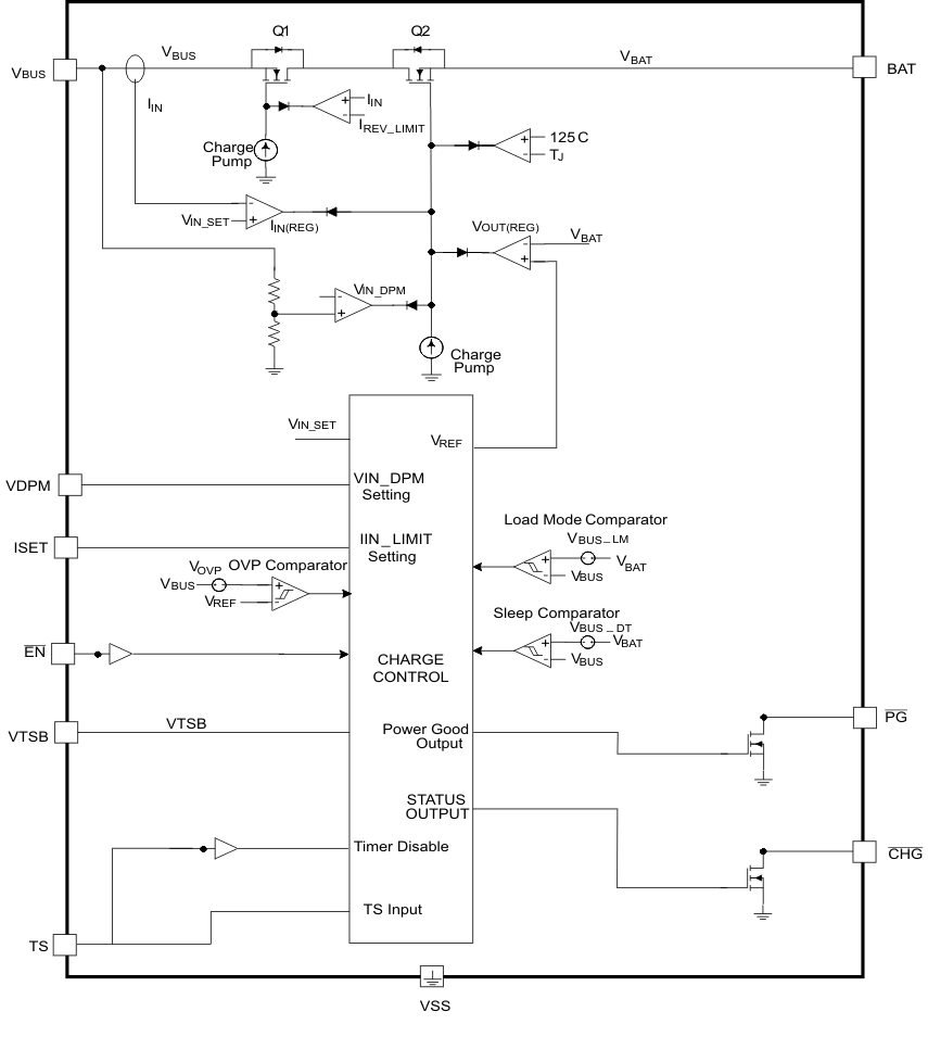
8.2 Functional Block Diagram
8.3 Feature Description
8.3.1 Input Voltage-Based Dynamic Power Management (VBUS-DPM)
The VBUS-DPM feature is used to detect an input source voltage that is reaching its current limit due to excessive load and causing the voltage to reduce. When the input voltage drops to the VBUS-DPM threshold the internal pass FET reduces the current until there is no further drop in voltage at the input. This prevents a source with voltage less than VBUS-DPM to power the BAT pin. This unique feature makes the IC work well with current limited (for example, high impedance) power sources, such as solar panels or inductive changing pads. This is also an added safety feature that helps protect the source from excessive loads.
An external resistor is used to program the VBUS_DPM. The programming resistor, RVDPM is dictated by the following equation:
where
- VBUS_DPM is the desired input voltage regulation voltage threshold;
- VBUS_DPM_1 is the built in offset threshold, typically 3.5 V
- KVBUS_DPM is a gain factor found in the electrical specification.
If VDPM pin is shorted to VSS, the VBUS_DPM is set to typically 3.65 V.
If the VDPM pin is floated (open circuit), the IC operates in battery tracking mode. In this case, VBUS DPM threshold is internally set as VTRK, which is typically BAT+100 mV (BAT>3.65 V) or 3.75 V (BAT≤3.4 V).
8.3.2 CHG Pin Indication
The charge pin has an internal open drain FET which is on (pulls down to VSS) during the first charge only (unless TS pin is tied to VTSB pin) and is turned off once the battery reaches voltage regulation and the charge current tapers to the internally set termination threshold.
The charge pin is high impedance in sleep mode and OVP (if PG is high impedance) and return to its previous state once the condition is removed.
Cycling input power, toggling EN pin, or releasing or entering pre-charge mode causes the CHG pin to go low if power is good and a discharged battery is attached. This is considered the start of a first charge cycle.
8.3.3 CHG and PG LED Pull-Up Source
For host monitoring, a pullup resistor is used between the STATUS pin and the VCC of the host. For a visual indication a resistor in series with an LED is connected between the STATUS pin and a power source. If the CHG or PG source is capable of exceeding 7 V, a 6.2-V Zener diode should be used to clamp the voltage. If the source is the BAT pin, note that as the battery changes voltage, the brightness of the LEDs vary.
Table 1. CHG
| CHARGING STATE | CHG FET/LED (VTS< VLP(TS)) | CHG FET/LED (VTS> VLP(TS)) |
|---|---|---|
| 1st Charge | ON | ON |
| Refresh Charge | OFF | ON |
| OVP | OFF | |
| Sleep | OFF | |
| TEMP Fault | ON for 1st Charge | ON |
| Charge when BAT< BAT(SC) | OFF | ON |
Table 2. PG
| INPUT POWER GOOD STATE | PG FET/LED |
|---|---|
| Normal Input (BAT+VBUS_DT<VBUS<VOVP) and (VBUSDPM<VBUS<VOVP) |
ON |
| UVLO | OFF |
| Sleep Mode | |
| OVP Mode | |
| PG is independent of chip disable | |
8.3.4 Power Good Indication (PG)
After a source is applied to VBUS and the voltage rises above the UVLO and sleep thresholds (VBUS>BAT+VBUS-DT) and VBUS-DPM threshold (VBUS_DPM or VTRK), but is less than OVP (VBUS<VOVP), then the PG FET turns on and provides a low impedance path to ground. The EN pin state does not affect this functionality.
8.4 Device Functional Modes
8.4.1 Power-Down or Undervoltage Lockout (UVLO)
The IC is in power down mode if the VBUS and BAT pin voltages are both less than UVLO. The part is considered "dead" and all the pins are high impedance. Once the VBUS voltage rises above the UVLO threshold the IC enters sleep mode or an active mode depending on control pin status and the BAT pin (battery) voltage.
8.4.2 Operation Mode Detection and Transition
On power up (VBUS or BAT ramps up, or EN pin changes status), the IC performs operation mode detection to identify the operation mode based on the VBUS voltage, battery voltage, load current, and control pin status.
Two comparators are needed for the detection, load mode comparator and sleep mode comparator.
When VBUS falls below the lower limit of the load mode comparator, the IC goes to load mode; when VBUS is above the upper limit of the sleep comparator, the IC goes to charge mode, as shown in Figure 4.
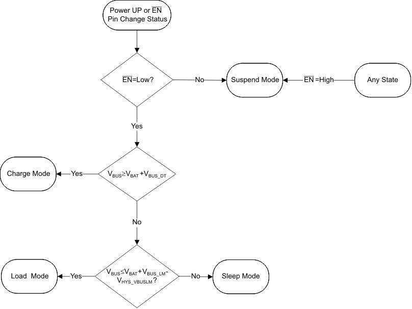 Figure 4. Operation Mode Detection Flow Chart
During load mode, when VBUS is above upper limit of load mode and the load current is below the minimum load current (ILM_MIN), the IC stays in load mode for a deglitch time of 100 mS and then goes to sleep mode.
If VBUS is above the upper limit of the sleep comparator during this period, after 45-µs deglitch time, the IC stops load mode and goes into the charge mode. The maximum current to the battery is limited by the FET RDSon during this transition.
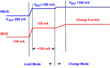 Figure 5. Sleep Comparator Operation
During charge mode, if VBUS falls to the lower limit of sleep comparator, the IC goes to sleep mode after a deglitch time of 32 mS. If VBUS falls faster than 32 ms to below the lower limit of load mode comparator, the IC goes to load mode after a deglitch time of 32 ms, as shown in Figure 6.
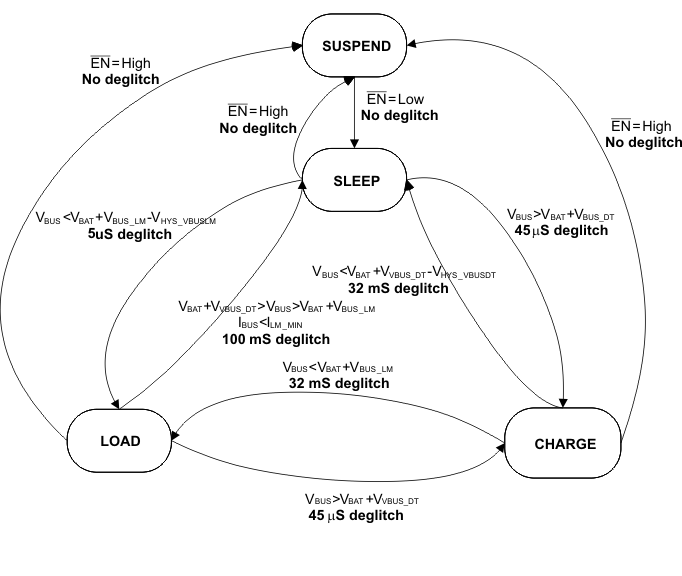 Figure 6. Operation Mode Transition Diagram
In load mode, if the load is higher than ILM_MIN, or the voltage at VBUS pin is lower than upper limit of load mode comparator, load mode is continuous.
If the load is smaller than ILM_MIN in load mode, and VBUS is higher than the upper limit, then the IC goes to sleep mode after deglitch time of 100 mS. In sleep mode, once VBUS drops lower than the lower limits of the load mode comparator, the IC goes to load mode again. In this case, the above process repeats, and IC keeps changing operations mode (between sleep mode and load mode). The mode change frequency is less than 10 Hz, and VBUS has a ripple of 150 mV.
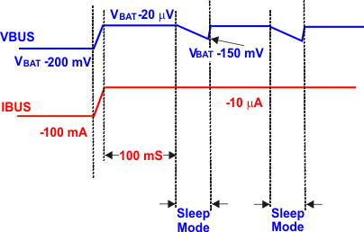 Figure 7. Load Mode Operation
8.4.3 Sleep Mode
If the VBUS pin voltage is below the BAT voltage and above the UVLO threshold, the charge current is disabled, the safety timer counting pauses (not reset) and the PG and CHG pins are high impedance. As the input voltage rises and the charger exits sleep mode, the PG pin goes low, the safety timer continues to count, charge is enabled, and the CHG pin remains high impedance until current flows out the BAT pin.
8.4.4 Load Mode
Load mode is used when the charging source is removed and an external accessory needs power from the battery.
To start the load mode, the minimum BAT pin voltage is BAT_REV_ST. When load mode is active, the oscillator and charge pump will operate at reduced speed to reduce quiescent current prolonging battery life.
During load mode, reverse current is monitored, and once it rises to an internally set threshold, IREV_LIMIT, the load current regulation loop will limit the load current to the threshold for a blanking time of tREV_LIMIT_BLK. If the overload condition continues after the blanking time of tREV_LIMIT_BLK, the load current limit threshold will be reduced to IREV_LIMIT_BK (about 50mA) and load mode continues, until the VBUS drops below UVLO or other failure occurs. If the load current drops below IREV_LIMIT_BK, the load current limit will be set back to IREV_LIMIT after a delay of tREV_LIMIT_REC, as shown in Figure 8.
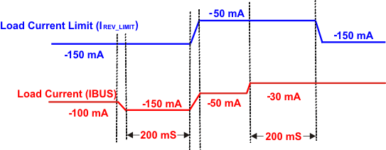 Figure 8. Load Current Limiting
8.4.5 Charge Mode
8.4.5.1 Overvoltage Protection (OVP) – Continuously Monitored
If the input source applies an overvoltage, the pass FET, if previously on, turns off after a deglitch, tBLK(OVP). The timer ends and the CHG and PG pins go to a high impedance state. Once the overvoltage returns to a normal voltage and after a deglitch time of tDGL(PG_OVP) , the PG pin goes low, timer continues, charge continues, and the CHG pin goes low after a 25-ms deglitch.
8.4.5.2 Power Up
The IC is alive after the VBUS or BAT voltage ramps above UVLO (see sleep mode), the IC resets all logic and timers, and starts to perform many of the continuous monitoring routines. Typically the input voltage quickly rises through the UVLO and sleep states where the IC declares power good, starts the safety timer, enables the CHG pin, and starts the normal charge routine.
8.4.5.3 Battery Detect Routine
The battery detect routine checks for a missing battery while keeping the BAT pin at a useable voltage. Whenever the battery is missing, the CHG pin is high impedance.
The battery detect routine is run when entering and exiting LPCM to verify if battery is present, or run all the time if battery is missing. On power-up, if battery voltage is greater than VRCH threshold, a battery detect routine is run to determine if a battery is present.
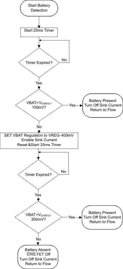 Figure 9. Battery Detection Flow Chart
8.4.5.4 New Charge Cycle
A new charge cycle is started when a good power source is applied, when performing a charge disable/enable (EN), when exiting limited power charge mode (LPCM), when detecting a battery insertion, or when the BAT voltage dropping below the VRCH threshold. The CHG pin is active low only during the first charge cycle, therefore exiting LPCM or dropping below VRCH will not turn on the CHG pin FET, if the CHG pin is already high impedance.
8.4.5.5 BAT Output
The charger’s BAT pin provides current (IOUT) to the battery and to the system, if present. This IC can be used to charge the battery plus power the system or charge just the battery assuming the loads do not exceed the available current. The BAT pin is a current limited source and is inherently protected against shorts. If the system load ever exceeds the output programmed current threshold, the output voltage will drop unless there is sufficient capacitance or a charged battery present to supplement the excessive load. If the voltage on BAT drops below the pre-charge to fast-charge threshold, Vlowv= 2.5 V typical, IOUT is reduced to 10% typical of the fast charge current .
8.4.5.6 Fast Charge Current (IOUT)
An external resistor on the ISET pin is used to program the output current (50 to 800mA) and can be used as a current monitor.
where
- IOUT is the desired fast charge current in amps;
- KISET is a gain factor found in the electrical specification, typically 395 AΩ
The ISET resistor is short protected and will detect a resistance lower than RISET_MAX. The detection requires at least 80mA of output current. If a short is detected, then the IC will latch off and can only be reset by cycling the power. The BAT current is internally clamped to a maximum current IOUT_CL which is independent of the ISET short detection circuitry.
8.4.5.7 Termination
Once the BAT pin goes above VRCH (reaches voltage regulation), and the current tapers down to the termination threshold (20% of the fast charge current), the CHG pin goes high impedance, and a battery detect route is run to determine if the battery was removed or the battery is full. If the battery is present, the charge current will terminate. If the battery was removed along with the thermister, then the TS pin is driven high and the charger enters LPCM. If the battery was removed and the TS pin is held in the active region, then the battery detect routine will continue until a battery is inserted. After termination, if the BAT pin voltage drops to VRCH (100mV below regulation) while input power remains applied then a new charge is initiated, but the CHG pin remains at a high impedance (off). The termination threshold is raised by 14%, for the first minute of a charge cycle so if a full battery is removed and reinserted or a new charge cycle is initiated, that the new charge terminates (less than 1 minute). Batteries that have relaxed many hours may take several minutes to taper to the termination threshold and terminate charge.
8.4.5.8 Timers
The pre-charge timer is set to 30 minutes. The fast charge timer is fixed at 10 hours and can be increased real time by going into thermal regulation or VBUS_DPM. While in thermal regulation or VBUS_DPM, the timer clock slows by a factor of 2, resulting in a clock than counts half as fast which will increase the total time. If either the 30 minute or ten hour timer times out, the charging is terminated and the CHG pin goes high impedance if not already in that state. The timer is reset by disabling the IC, cycling power, or going into and out of LPCM.
8.4.5.9 Battery Temperature Monitoring
When connected to a thermistor that monitors the battery's temperature, the TS feature prevents battery damage by reducing charge current or voltage at battery temperature extremes. The TS feature is designed to be compatible with the JEITA temperature standard for Li-Ion batteries. There are four thresholds, 60°C, 45°C, 10°C, and 0°C. Normal operation occurs between 10°C and 45°C. If between 0°C and 10°C, the charge current level is cut in half and if between 45°C and 60°C, the regulation voltage is reduced to 4.1Vmax.
The voltage based TS sensing is used due to the flexibility to be compatible with different NTCs. VTSB is used as the voltage reference for TS sensing, and two external TS voltage divider (RT1 and RTH) are used to set the targeted temperature threshold. Above 60°C or below 0°C the charge is disabled.
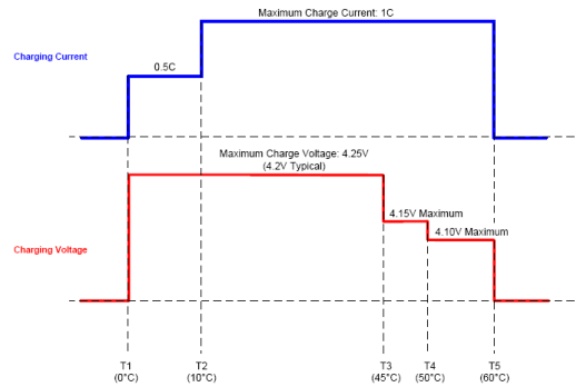 Figure 10. Charge JEITA Profile
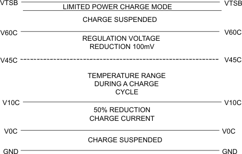 Figure 11. TS Pin, Thermister Sense Thresholds
Assuming a 103AT NTC thermister on the battery pack as shown in Figure 13, the value RT1 can be determined by using the following equation (select the most critical temperature for the best precision):

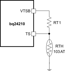 Figure 12. TS Resistor Network
The TS pin has another additional feature. When the TS pin is driven high (VTS> VLP(TS)), the IC operates in limited power charge mode.
8.4.5.10 Limited Power Charge Mode – TS Pin High
When the TS pin goes high to the limited power charge mode (LPCM) threshold (VLP(TS)), the part enters limited power charge mode. This mode is used normally for solar charging applications or other high impedance input sources that desire to modify the termination routine and other timers. When entering the limited power charging mode, the pre-charge timer and 10 hour safety timer is held in reset, and the termination routine is modified. A battery detect routine is run to see if the battery was removed or not. If the battery was removed then the CHG pin will go to its high impedance state if not already there. If a battery is detected, the normal charge process begins. If the normal termination conditions are met (Icharge<ITERM, BAT>VRCH) and VBUS_DPM loop is not active, the charging process terminates, and the CHG pin goes to its high impedance state if not already there. When the regular timers are disabled there still is a 2 hour timer if the part is stuck in DPM above 4.1 V but outside of termination conditions at which point charging will terminate and re-start if the voltage falls below 4.1V.
When coming out of the limited power charging mode, the battery detect routine is run and if a battery is detected, then a new charge cycle begins and the CHG LED turns on.
Limited power charge mode is not necessary for all solar charging. A solar panel charging in normal mode without TS pulled high would keep the normal termination timers active and would allow the TS temperature monitoring functions to be used.
If limited power charging mode is not desired upon removal of the battery with a thermister, apply a voltage equal to 30% VTSB on TS pin using two external resistors to set a voltage divider and disable the TS monitor function.
8.4.6 Suspend Mode
When EN pin is pulled to HIGH level, the IC operates in suspend mode, with Q1 and Q2 OFF and very low leakage current into and between VBUS and BAT pins. The PG pin continues to operate to indicate a good power source even while in suspend mode.