ZHCS384H November 2011 – July 2022 BQ24160 , BQ24160A , BQ24161 , BQ24161B , BQ24163 , BQ24168
PRODUCTION DATA
- 1 特性
- 2 应用
- 3 说明
- 4 Revision History
- 5 Device Comparison Table
- 6 Pin Configuration and Functions
- 7 Specifications
-
8 Detailed Description
- 8.1 Overview
- 8.2 Functional Block Diagram
- 8.3
Feature Description
- 8.3.1 Charge Mode Operation
- 8.3.2 Battery Charging Process
- 8.3.3 Battery Detection
- 8.3.4 Dynamic Power Path Management (DPPM)
- 8.3.5 Input Source Connected
- 8.3.6 Battery Only Connected
- 8.3.7 Battery Discharge FET (BGATE)
- 8.3.8 DEFAULT Mode
- 8.3.9 Safety Timer and Watchdog Timer (BQ24160/BQ24161/BQ24161B/BQ24163 only)
- 8.3.10 D+, D– Based Adapter Detection for the USB Input (D+, D–, BQ24160/0A/3)
- 8.3.11 USB Input Current Limit Selector Input (PSEL, BQ24161/161B/168 only)
- 8.3.12 Hardware Chip Disable Input (CD)
- 8.3.13 LDO Output (DRV)
- 8.3.14 External NTC Monitoring (TS)
- 8.3.15 Thermal Regulation and Protection
- 8.3.16 Input Voltage Protection in Charge Mode
- 8.3.17 Charge Status Outputs (STAT, INT)
- 8.3.18 Good Battery Monitor
- 8.4 Device Functional Modes
- 8.5 Programming
- 8.6
Register Maps
- 8.6.1 Status/Control Register (READ/WRITE)
- 8.6.2 Battery/ Supply Status Register (READ/WRITE)
- 8.6.3 Control Register (READ/WRITE)
- 8.6.4 Control/Battery Voltage Register (READ/WRITE)
- 8.6.5 Vender/Part/Revision Register (READ only)
- 8.6.6 Battery Termination/Fast Charge Current Register (READ/WRITE)
- 8.6.7 VIN-DPM Voltage/ DPPM Status Register
- 8.6.8 Safety Timer/ NTC Monitor Register (READ/WRITE)
- 9 Application and Implementation
- 10Power Supply Recommendations
- 11Layout
- 12Device and Documentation Support
封装选项
机械数据 (封装 | 引脚)
散热焊盘机械数据 (封装 | 引脚)
- RGE|24
订购信息
8.3.14 External NTC Monitoring (TS)
The I2C interface allows the user to easily implement the JEITA standard for systems where the battery pack thermistor is monitored by the host. Additionally, the BQ2416xx provides a flexible, voltage based TS input for monitoring the battery pack NTC thermistor. The voltage at TS is monitored to determine that the battery is at a safe temperature during charging. The BQ24160, BQ24160A, BQ24161B, BQ24163, and BQ24168 enable the user to easily implement the JEITA standard for charging temperature while the BQ24161 only monitors the hot and cold cutoff temperatures and leaves the JEITA control to the host. The JEITA specification is shown in.
 Figure 8-4 Charge
Current During TS Conditions
Figure 8-4 Charge
Current During TS ConditionsTo satisfy the JEITA requirements, four temperature thresholds are monitored; the cold battery threshold (TNTC < 0°C), the cool battery threshold (0°C < TNTC < 10°C), the warm battery threshold (45°C < TNTC ≤ 60°C) and the hot battery threshold (TNTC > 60°C). These temperatures correspond to the VCOLD, VCOOL, VWARM, and VHOT thresholds. Charging is suspended and timers are suspended when VTS < VHOT or VTS > VCOLD. When VWARM > VTS > VHOT, the battery regulation voltage is reduced by 140 mV from the programmed regulation threshold. When VCOLD > VTS > VCOOL, the charging current is reduced to half of the programmed charge current.
The TS function is voltage based for maximum flexibility. Connect a resistor divider from DRV to GND with TS connected to the center tap to set the threshold. The connections are shown in Figure 8-11. The resistor values are calculated using the following equations:
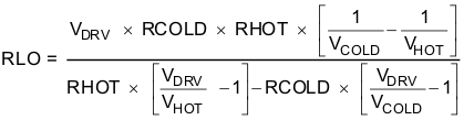
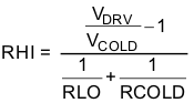
Where:
VCOLD = 0.60 × VDRV
VHOT = 0.30 × VDRV
Where RHOT is the NTC resistance at the hot temperature and RCOLD is the NTC resistance at cold temperature.
For the BQ24160, BQ24161B, BQ24163, and BQ24168, the WARM and COOL thresholds are not independently programmable. The COOL and WARM NTC resistances for a selected resistor divider are calculated using the following equations:


 Figure 8-5 TS Circuit