ZHCS384H November 2011 – July 2022 BQ24160 , BQ24160A , BQ24161 , BQ24161B , BQ24163 , BQ24168
PRODUCTION DATA
- 1 特性
- 2 应用
- 3 说明
- 4 Revision History
- 5 Device Comparison Table
- 6 Pin Configuration and Functions
- 7 Specifications
-
8 Detailed Description
- 8.1 Overview
- 8.2 Functional Block Diagram
- 8.3
Feature Description
- 8.3.1 Charge Mode Operation
- 8.3.2 Battery Charging Process
- 8.3.3 Battery Detection
- 8.3.4 Dynamic Power Path Management (DPPM)
- 8.3.5 Input Source Connected
- 8.3.6 Battery Only Connected
- 8.3.7 Battery Discharge FET (BGATE)
- 8.3.8 DEFAULT Mode
- 8.3.9 Safety Timer and Watchdog Timer (BQ24160/BQ24161/BQ24161B/BQ24163 only)
- 8.3.10 D+, D– Based Adapter Detection for the USB Input (D+, D–, BQ24160/0A/3)
- 8.3.11 USB Input Current Limit Selector Input (PSEL, BQ24161/161B/168 only)
- 8.3.12 Hardware Chip Disable Input (CD)
- 8.3.13 LDO Output (DRV)
- 8.3.14 External NTC Monitoring (TS)
- 8.3.15 Thermal Regulation and Protection
- 8.3.16 Input Voltage Protection in Charge Mode
- 8.3.17 Charge Status Outputs (STAT, INT)
- 8.3.18 Good Battery Monitor
- 8.4 Device Functional Modes
- 8.5 Programming
- 8.6
Register Maps
- 8.6.1 Status/Control Register (READ/WRITE)
- 8.6.2 Battery/ Supply Status Register (READ/WRITE)
- 8.6.3 Control Register (READ/WRITE)
- 8.6.4 Control/Battery Voltage Register (READ/WRITE)
- 8.6.5 Vender/Part/Revision Register (READ only)
- 8.6.6 Battery Termination/Fast Charge Current Register (READ/WRITE)
- 8.6.7 VIN-DPM Voltage/ DPPM Status Register
- 8.6.8 Safety Timer/ NTC Monitor Register (READ/WRITE)
- 9 Application and Implementation
- 10Power Supply Recommendations
- 11Layout
- 12Device and Documentation Support
封装选项
机械数据 (封装 | 引脚)
散热焊盘机械数据 (封装 | 引脚)
- RGE|24
订购信息
8.3.5 Input Source Connected
When a valid input source is connected to IN or USB and the BQ2416xx is NOT in High Impedance mode, the buck converter enters soft-start and turns on to power the load on SYS. The STAT/INT pin outputs a 128-µs interrupt pulse to alert the host that an input has been connected. The FAULT bits indicate a normal condition, and the Supply Status register indicates that a new supply is connected. The CE bit (bit 1) in the control register (0x02) indicates whether a charge cycle is initiated. By default, the BQ2416xx ( CE = 0) enables a charge cycle when a valid input source is connected. When the CE bit is '1' and a valid input source is connected, the battery FET is turned off and the SYS output is regulated to the VSYS(REG) programmed by the VBATREG threshold in the I2C register. A charge cycle is initiated when the CE bit is written to a 0 value (cleared).
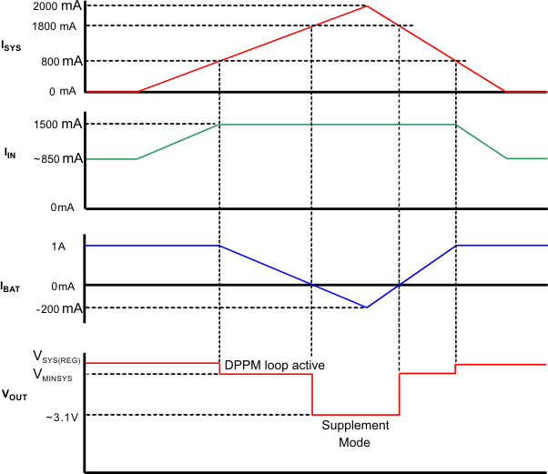
When the CE bit is a 0 and a valid source is connected to IN or USB, the buck converter starts up using soft-start. A charge cycle is initiated 64 ms after the buck converter iniates startup. When VBAT is high enough that VSYS > VSYS(REG), the battery FET is turned on and the SYS output is connected to BAT. If the SYS voltage falls to VSYS(REG), it is regulated to that point to maintain the system output even with a deeply discharged or absent battery. In this mode, the SYS output voltage is regulated by the buck converter and the battery FET linearly regulates the charge current into the battery. The current from the supply is shared between charging the battery and powering the system load at SYS. The dynamic power-path management (DPPM) circuitry of the BQ2416xx monitors the current limits continuously, and if the SYS voltage falls to the VMINSYS voltage, it adjusts charge current to maintain the minimum system voltage and supply the load on SYS. If the charge current is reduced to zero and the load increases further, the BQ2416xx enters battery-supplement mode. During supplement mode, the battery FET is turned on and the battery supplements the system load.
When an input is connected with no battery attached and termination enabled, the startup process proceeds as normal until the termination deglitch times out. After this, the BQ2416xx enters battery detection and waits for a battery to be connected. Once a battery is connected and passes battery detection, a new charge cycle begins. Once the battery is applied, the HZMODE bit or CD pin must be toggled before writing the BATREG to a higher voltage and beginning a new charge cycle. Failure to do this can result in SYS unexpectedly regulating to 15% above VBATREG.
 Figure 8-2 Example DPPM Response
(VSupply = 5 V, VBAT = 3.1 V, 1.5 A Input Current
Limit)