ZHCS384H November 2011 – July 2022 BQ24160 , BQ24160A , BQ24161 , BQ24161B , BQ24163 , BQ24168
PRODUCTION DATA
- 1 特性
- 2 应用
- 3 说明
- 4 Revision History
- 5 Device Comparison Table
- 6 Pin Configuration and Functions
- 7 Specifications
-
8 Detailed Description
- 8.1 Overview
- 8.2 Functional Block Diagram
- 8.3
Feature Description
- 8.3.1 Charge Mode Operation
- 8.3.2 Battery Charging Process
- 8.3.3 Battery Detection
- 8.3.4 Dynamic Power Path Management (DPPM)
- 8.3.5 Input Source Connected
- 8.3.6 Battery Only Connected
- 8.3.7 Battery Discharge FET (BGATE)
- 8.3.8 DEFAULT Mode
- 8.3.9 Safety Timer and Watchdog Timer (BQ24160/BQ24161/BQ24161B/BQ24163 only)
- 8.3.10 D+, D– Based Adapter Detection for the USB Input (D+, D–, BQ24160/0A/3)
- 8.3.11 USB Input Current Limit Selector Input (PSEL, BQ24161/161B/168 only)
- 8.3.12 Hardware Chip Disable Input (CD)
- 8.3.13 LDO Output (DRV)
- 8.3.14 External NTC Monitoring (TS)
- 8.3.15 Thermal Regulation and Protection
- 8.3.16 Input Voltage Protection in Charge Mode
- 8.3.17 Charge Status Outputs (STAT, INT)
- 8.3.18 Good Battery Monitor
- 8.4 Device Functional Modes
- 8.5 Programming
- 8.6
Register Maps
- 8.6.1 Status/Control Register (READ/WRITE)
- 8.6.2 Battery/ Supply Status Register (READ/WRITE)
- 8.6.3 Control Register (READ/WRITE)
- 8.6.4 Control/Battery Voltage Register (READ/WRITE)
- 8.6.5 Vender/Part/Revision Register (READ only)
- 8.6.6 Battery Termination/Fast Charge Current Register (READ/WRITE)
- 8.6.7 VIN-DPM Voltage/ DPPM Status Register
- 8.6.8 Safety Timer/ NTC Monitor Register (READ/WRITE)
- 9 Application and Implementation
- 10Power Supply Recommendations
- 11Layout
- 12Device and Documentation Support
封装选项
机械数据 (封装 | 引脚)
散热焊盘机械数据 (封装 | 引脚)
- RGE|24
订购信息
9.2.2.1 Output Inductor and Capacitor Selection Guidelines
When selecting an inductor, several attributes must be examined to find the right part for the application. First, the inductance value should be selected. The BQ2416xx is designed to work with 1.5-µH to 2.2-µH inductors. The chosen value will have an effect on efficiency and package size. Due to the smaller current ripple, some efficiency gain is reached using the 2.2-µH inductor, however, due to the physical size of the inductor, this may not be a viable option. The 1.5-µH inductor provides a good tradeoff between size and efficiency.
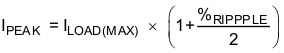
Once the inductance has been selected, the peak current must be calculated in order to choose the current rating of the inductor. Use Equation 5 to calculate the peak current.
The inductor selected must have a saturation current rating greater than or equal to the calculated IPEAK. Due to the high currents possible with the BQ2416xx, a thermal analysis must also be done for the inductor. Many inductors have a 40°C temperature-rise rating. The DC component of the current can cause a 40°C temperature rise above the ambient temperature in the inductor. For this analysis, the typical load current may be used adjusted for the duty cycle of the load transients. For example, if the application requires a 1.5-A DC load with peaks at 2.5 A 20% of the time, a Δ40°C temperature rise current must be greater than 1.7 A:

The BQ2416xx provides internal loop compensation. Using this scheme, the BQ2416xx is stable with 10 µF to 200 µF of local capacitance on the SYS output. The capacitance on the SYS rail can be higher if distributed amongst the rail. To reduce the output voltage ripple, a ceramic capacitor with the capacitance between 10 µF and 47 µF is recommended for local bypass to SYS. A 47-µF bypass capacitor is recommended for optimal transient response.