ZHCSAF0E September   2012  – January 2018

PRODUCTION DATA.  

  1. 特性
  2. 应用范围
  3. 说明
    1.     典型应用电路
  4. 修订历史记录
  5. 说明 (续)
  6. Device Comparisons
  7. Pin Configuration and Functions
    1.     Pin Functions
  8. Specifications
    1. 8.1 Absolute Maximum Ratings
    2. 8.2 ESD Ratings
    3. 8.3 Recommended Operating Conditions
    4. 8.4 Thermal Information
    5. 8.5 Electrical Characteristics
    6. 8.6 Timing Requirements
    7. 8.7 Typical Characteristics
  9. Detailed Description
    1. 9.1 Overview
    2. 9.2 Functional Block Diagrams
    3. 9.3 Operational Flow Chart
    4. 9.4 Feature Description
      1. 9.4.1 Input Voltage Protection
        1. 9.4.1.1 Input Overvoltage Protection
        2. 9.4.1.2 Bad Adaptor Detection/Rejection
        3. 9.4.1.3 Sleep Mode
        4. 9.4.1.4 Input Voltage Based DPM (Special Charger Voltage Threshold)
      2. 9.4.2 Battery Protection
        1. 9.4.2.1 Output Overvoltage Protection
        2. 9.4.2.2 Battery Detection at Power Up in DEFAULT Mode
        3. 9.4.2.3 Battery Short Protection
        4. 9.4.2.4 Battery Detection in Host Mode
      3. 9.4.3 DEFAULT Mode
      4. 9.4.4 USB Friendly Power Up
      5. 9.4.5 Input Current Limiting At Power Up
    5. 9.5 Device Functional Modes
      1. 9.5.1 Charge Mode Operation
        1. 9.5.1.1 Charge Profile
      2. 9.5.2 PWM Controller in Charge Mode
      3. 9.5.3 Battery Charging Process
      4. 9.5.4 Thermal Regulation and Protection
      5. 9.5.5 Charge Status Output, STAT Pin
      6. 9.5.6 Control Bits in Charge Mode
        1. 9.5.6.1 CE Bit (Charge Mode)
        2. 9.5.6.2 RESET Bit
        3. 9.5.6.3 OPA_Mode Bit
      7. 9.5.7 Control Pins in Charge Mode
        1. 9.5.7.1 CD Pin (Charge Disable)
      8. 9.5.8 BOOST Mode Operation
        1. 9.5.8.1 PWM Controller in Boost Mode
        2. 9.5.8.2 Boost Start Up
        3. 9.5.8.3 PFM Mode at Light Load
        4. 9.5.8.4 Protection in Boost Mode
          1. 9.5.8.4.1 Output Overvoltage Protection
          2. 9.5.8.4.2 Output Overload Protection
          3. 9.5.8.4.3 Battery Overvoltage Protection
        5. 9.5.8.5 STAT Pin in Boost Mode
      9. 9.5.9 High Impedance (Hi-Z) Mode
    6. 9.6 Programming
      1. 9.6.1 Serial Interface Description
        1. 9.6.1.1 F/S Mode Protocol
        2. 9.6.1.2 H/S Mode Protocol
        3. 9.6.1.3 I2C Update Sequence
        4. 9.6.1.4 Slave Address Byte
        5. 9.6.1.5 Register Address Byte
    7. 9.7 Register Description
  10. 10Application and Implementation
    1. 10.1 Application Information
      1. 10.1.1 Typical Application
        1. 10.1.1.1 Design Requirements
        2. 10.1.1.2 Detailed Design Procedure
      2. 10.1.2 Charge Current Sensing Resistor Selection Guidelines
      3. 10.1.3 Output Inductor and Capacitance Selection Guidelines
    2. 10.2 Typical Performance Curves
  11. 11Power Supply Recommendations
    1. 11.1 System Load After Sensing Resistor
      1. 11.1.1 The Advantages:
      2. 11.1.2 Design Requirements and Potential Issues:
  12. 12Layout
    1. 12.1 Layout Guidelines
    2. 12.2 Layout Example
  13. 13Device and Documentation Support
    1. 13.1 Documentation Support
      1. 13.1.1 Third-Party Products Disclaimer
    2. 13.2 接收文档更新通知
    3. 13.3 Community Resources
    4. 13.4 商标
    5. 13.5 静电放电警告
    6. 13.6 Glossary
  14. 14机械、封装和可订购信息
    1. 14.1 封装概要
      1. 14.1.1 芯片级封装尺寸

封装选项

机械数据 (封装 | 引脚)
散热焊盘机械数据 (封装 | 引脚)
订购信息

Charge Profile

Once a good battery with voltage below the recharge threshold has been inserted and a good adapter is attached, the bq24157 enters charge mode. In charge mode, the IC has five control loops to regulate input voltage, input current, charge current, charge voltage and device junction temperature. During the charging process, all five loops are enabled and the one that is dominant takes control. The IC supports a precision Li-ion or Li-polymer charging system for single-cell applications. Figure 17 (a) indicates a typical charge profile without input current regulation loop. It is the traditional CC/CV charge curve, while Figure 17(b) shows a typical charge profile when input current limiting loop is dominant during the constant current mode. In this case, the charge current is higher than the input current so the charge process is faster than the linear chargers. The input voltage threshold for DPM loop, input current limits, charge current, termination current, and charge voltage are all programmable using I2C interface.
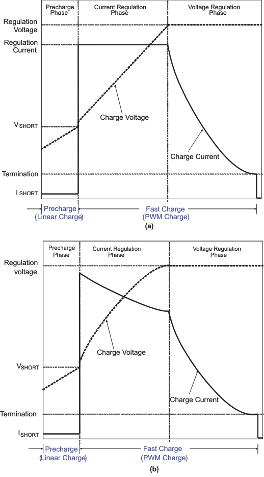
bq24157 typ_chg_pro_lus931.gifFigure 17. Typical Charging Profile for (a) without Input Current Limit, and (b) with Input Current Limit