ZHCSK78A september 2019 – august 2023 BQ21061
PRODUCTION DATA
- 1
- 1 特性
- 2 应用
- 3 说明
- 4 Revision History
- 5 Pin Configuration and Functions
- 6 Specifications
-
7 Detailed Description
- 7.1 Overview
- 7.2 Functional Block Diagram
- 7.3
Feature Description
- 7.3.1 Linear Charger and Power Path
- 7.3.2 Protection Mechanisms
- 7.3.3 VDD LDO
- 7.3.4 Load Switch/LDO Output and Control
- 7.3.5 PMID Power Control
- 7.3.6 System Voltage (PMID) Regulation
- 7.3.7 MR Wake and Reset Input
- 7.3.8 14-Second Watchdog for HW Reset
- 7.3.9 Faults Conditions and Interrupts ( INT)
- 7.3.10 Power Good ( PG) Pin
- 7.3.11 External NTC Monitoring (TS)
- 7.3.12 I2C Interface
- 7.4 Device Functional Modes
- 7.5 Register Map
- 8 Application and Implementation
- 9 Power Supply Recommendations
- 10Layout
- 11Device and Documentation Support
- 12Mechanical, Packaging, and Orderable Information
7.3.7.1 MR Wake or Short Button Press Functions
There are two programmable wake or short button press timers, WAKE1 and WAKE2. When the MR pin is held low for tWAKE1 the device sends an interrupt (128 µs active low pulse in the INT pin) and sets the MRWAKE1_TIMEOUT flag when it expires. If the MR pin continues to be driven low after WAKE1 and the WAKE2 timer expires, the BQ21061 sends a second interrupt and sets the MRWAKE2_TIMOUT flag. WAKE1 is used as the timer to wake the device from ship mode. WAKE2’s only function is to send the interrupt and has no effect on other BQ21061 functions. These flags are not cleared until they have been read by the host. Note that interrupts are only sent when the flags are set and the flags must be cleared in order for another interrupt to be sent upon MR press. The timer durations can be set through the MR_WAKEx_TIMER bits in the MRCTRL Register section.
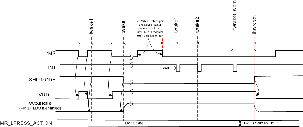
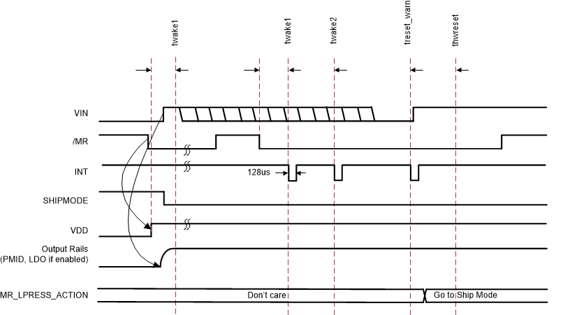
One of the main MR functions is to wake the device from Ship Mode when the MR is asserted. The device will exit the Ship Mode when the MR pin is held low for at least tWAKE1. Immediately after the MR is asserted, VDD will be enabled and the digital will start the WAKE counter. If the MR signal remains low until after the WAKE1 timer expires, the device will power up PMID and LDO (If enabled) completing the exit from the ship mode. If the MR signal goes high before the WAKE1 timer expires, the device will go back to the Ship Mode operation, never powering up PMID or the LDO. Note that if the MR pin remains low after exiting Ship Mode the wake interrupts will not be sent and the long button press functions like HW reset will not occur until the MR pin is toggled. In the case where a valid VIN (VIN > VUVLO) is connected prior to WAKE2 timer expiring, the device will exit the ship mode immediately regardless of the MR or wake timer state. Figure 7-3 and Figure 7-4 show these different scenarios.
 Figure 7-3 MR Wake from Ship Mode (MR_LPRESS_ACTION = Ship Mode, VIN not valid)
 Figure 7-4 MR Wake from Ship Mode – VIN Dependencies