ZHCSCA3 March 2014 AMC7832
PRODUCTION DATA.
- 1 特性
- 2 应用范围
- 3 说明
- 4 功率放大器偏置图表
- 5 修订历史记录
- 6 Terminal Configuration and Functions
-
7 Specifications
- 7.1 Absolute Maximum Ratings
- 7.2 Handling Ratings
- 7.3 Recommended Operating Conditions
- 7.4 Thermal Information
- 7.5 Electrical Characteristics
- 7.6 Timing Requirements - Serial Interface
- 7.7 Typical Characteristics: DAC
- 7.8 Typical Characteristics: ADC
- 7.9 Typical Characteristics: Reference
- 7.10 Typical Characteristics: Temperature Sensor
-
8 Detailed Description
- 8.1 Overview
- 8.2 Functional Block Diagram
- 8.3 Feature Description
- 8.4 Programming
- 8.5
Register Map
- 8.5.1 Interface Configuration: Address 0x00 - 0x02
- 8.5.2 Device Identification: Address 0x03 - 0x0D
- 8.5.3 Register Update (Buffered Registers): Address 0x0F
- 8.5.4 General Device Configuration: Address 0x10 - 0x17
- 8.5.5 DAC Clear And ALARMOUT Source Select: Address 0x1A - 0x1D
- 8.5.6 DAC Range: Address 0x1E
- 8.5.7 ADC Data: Address 0x20 - 0x41
- 8.5.8 DAC Data: Address 0x50 - 0x67
- 8.5.9 Status Registers: Address 0x70 - 0x72
- 8.5.10 Temperature And GPIO Data: Address 0x78 - 0x7A
- 8.5.11 Out-Of-Range ADC Thresholds: Address 0x80 - 0x93
- 8.5.12 Hysteresis: Address 0xA0 - 0xA5
- 8.5.13 Power-Down Registers: Address 0xB0 - 0xB3
- 8.5.14 ADC Trigger: Address 0xC0
- 9 Applications and Implementation
- 10Power Supply Recommendations
- 11Layout
- 12器件和文档支持
- 13机械封装和可订购信息
9 Applications and Implementation
9.1 Application Information
The AMC7832 device is a highly integrated, low-power, complete analog monitoring and control solution. Although the device can be used in many different systems -- Industrial Control, Test and Measurement, and Optical Communications -- the device is largely used in multi-channel RF communication driven applications which incorporate power amplifiers.
Power amplifiers (PAs) include transistor technologies that are extremely temperature sensitive, and require DC biasing circuits to optimize RF performance, power efficiency, and stability. The AMC7832 device provides 12 DAC channels, which can be used to bias the inputs of the power amplifiers. The device also includes an internal local temperature sensor, and 17 ADC channels for general-purpose monitoring.
There are mainly two different types of monitoring schemes: current sensing, and temperature sensing. In the current-sense application the PA drain current is monitored by measuring the shunt resistor’s differential voltage drop. The devices internal local temperature sensor and analog inputs – which can be configured for remote temperature ICs or thermistors – can be used to detect temperature variations during PA operation. Figure 57 shows the block diagrams to these different systems.
9.2 Typical Application
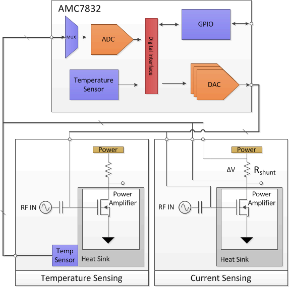 Figure 57. AMC7832 Example Control and Monitor System
9.2.1 Application Schematic
An example schematic incorporating the AMC7832 is listed in Figure 58.
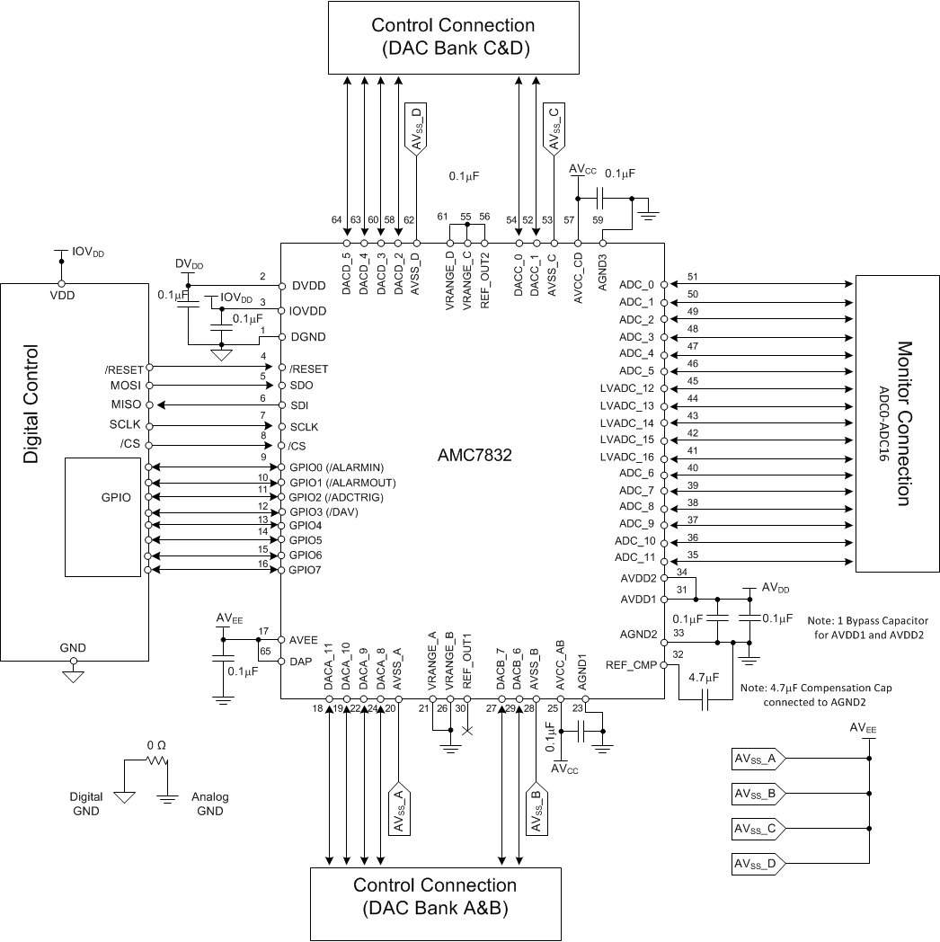 Figure 58. AMC7832 Example Schematic
9.2.2 Design Requirements
The AMC7832 Example Schematic uses most of the following design parameters.
Table 54. Design Parameters
| DESIGN PARAMETER | EXAMPLE VALUE | |
|---|---|---|
| AVCC AVEE IOVDD DVDD AVDD |
5V -12V 3.3V 5V 5V |
|
| ADC Bipolar inputs ADC Unipolar inputs |
(ADC0 – ADC11) (LV_ADC12 – LV_ADC16) |
-12.5 to +12.5-V input range 0 to +5-V range |
| DAC Output voltage Ranges | VRANGEA: GND VRANGEB: GND VRANGEC: 2.5V (REF_OUT2) VRANGED: 2.5V (REF_OUT2) |
[0 to +5-V Range] [0 to +5-V Range] [-10 to 0-V Range] [-10 to 0-V Range] |
| Remote temperature sensing | IC Temperature sensor (LM50) or thermistor | |
9.2.3 Detailed Design Procedure
The following displays a set of parameters and concepts that will facilitate the design process:
- AVCC and AVEE voltage values
- ADC input voltage range
- DAC Output voltage Ranges
- Remote temperature applications
9.2.3.1 ADC Input Conditioning
The AMC7832 has a single ADC core that features a multi-channel multiplexer input stage to a successive approximation register (SAR) ADC. The analog inputs are separated into two input classes: bipolar ADC inputs (high-voltage) and unipolar ADC Inputs (low-voltage). The high-voltage analog inputs (ADC_0 – ADC_11) feature a -12.5-V to +12.5-V input range, while the low-voltage analog inputs (LV_ADC12 – LV_ADC16) accept a full-scale range of 0 to 2 x VREF (VREF corresponds to a +2.5-V internal reference to the ADC block, and is externally available on the REF_CMP pin). For additional noise filtering, a 4.7-µF capacitor is recommended between the REF_CMP and GND. The value of this cap must exceed 470nF to ensure reference stability. A high-quality ceramic type NP0 or X7R is recommended for its optimal performance across temperature, and very low dissipation factor.
During conversion the input current per channel will vary with the total update time which is determined by the number and type of channels (NCH) and the conversion rate setting CONV-RATE in the ADC Configuration register (address 0x10). This information is displayed in Table 55.

Where:
CIN: Internal ADC input channel capacitance
ΔV : The maximum voltage difference between analog inputs
FS = f(CONVRATE, NCHBIPOLAR, NCHUNIPOLAR) = 1/TS
The total update time (TS) can be determined from Table 55.
Table 55. ADC Update Time per Input Channel
| CONV-RATE[1:0] | TS (μs) / CHANNEL UNIPOLAR INPUT CHANNEL |
TS (μs) / CHANNEL BIPOLAR INPUT CHANNEL |
TS (μs) TEMPERATURE SENSOR CHANNEL |
|---|---|---|---|
| 00 | 11.5 | 34.5 | 256 |
| 01 | 23 | 34.5 | 256 |
| 10 | 34.5 | 34.5 | 256 |
| 11 | 69 | 69 | 256 |
To reduce DC error in sampling, it is recommended to decrease the ADC input impedance and reduce any input capacitance to ground. Increasing the input capacitance essentially increases CIN, and therefore increases the required amount of input current (IIN).
In applications where the signal source has high impedance, it is recommended that the analog input is buffered before applying to the ADC channel.
Special care must be taken when biasing the two input classes, as both classes have different voltages – with respect to GND – that they cannot exceed. These voltage values are located in Absolute Maximum Ratings.
9.2.3.2 DAC Output Range Selection
The AMC7832 contains 12 DACs that are arranged by different DAC banks, where each channel within a bank shares a common programmable voltage range. Each DAC bank is fully programmable with up to three different voltage ranges: -10 to 0-V, 0 to +10-V, and 0 to +5-V. The VRANGE terminals combined with the DAC configuration register sets the different DAC voltage ranges.
The output buffer is capable of generating rail-to rail voltages on its output, giving an output range of AVSS to AVCC. The maximum source and sink capability of this internal amplifier is listed in the Electrical Characteristics DAC Output Characteristics.
The graphs listed in the Application plots section illustrate the relationship of both stability and settling time with different capacitive and resistive loading structures.
9.2.3.3 Temperature Sensing Applications
The AMC7832 contains one local temperature and 5 low-voltage unipolar channels that are easily configurable to remote temperature sensor circuits. The integrated temperature sensor and analog input registers automatically update with every conversion. An example of a remote temperature sensor connection is displayed in Figure 59.
The temperature sensor described is a LM50, a high precision integrated-circuit temperature sensor that can sense a -40°C to +125°C temperature range using a single positive supply. The full-scale output of the temperature sensor ranges from +100mV to +1.75V for a -40°C to +125°C temperature range. In an extremely noisy environment it may be necessary to add some filtering to minimize noise pickup. A typical recommended value for the bypass capacitor is 0.1µF from V+ to GND. A high-quality ceramic type NP0 or X7R is recommended for its optimal performance across temperature, and very low dissipation factor.
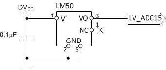 Figure 59. External Remote Temperature IC (LM50) Connected to AMC7832 (LV_ADC15) Input Pin
9.2.3.4 Application Curves
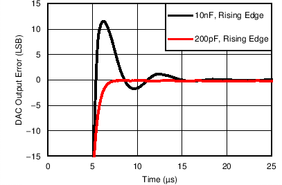
| T = 25°C, Code 0x400 to 0xC00 to within 1/2 LSB | ||
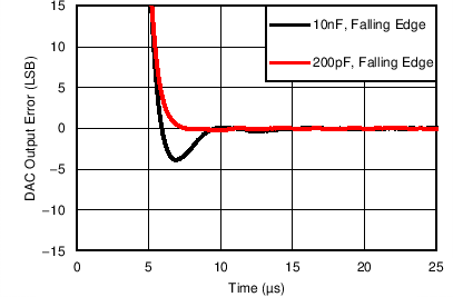
| T = 25°C, Code 0xC00 to 0x400 to within 1/2 LSB | ||