ZHCSCA3 March 2014 AMC7832
PRODUCTION DATA.
- 1 特性
- 2 应用范围
- 3 说明
- 4 功率放大器偏置图表
- 5 修订历史记录
- 6 Terminal Configuration and Functions
-
7 Specifications
- 7.1 Absolute Maximum Ratings
- 7.2 Handling Ratings
- 7.3 Recommended Operating Conditions
- 7.4 Thermal Information
- 7.5 Electrical Characteristics
- 7.6 Timing Requirements - Serial Interface
- 7.7 Typical Characteristics: DAC
- 7.8 Typical Characteristics: ADC
- 7.9 Typical Characteristics: Reference
- 7.10 Typical Characteristics: Temperature Sensor
-
8 Detailed Description
- 8.1 Overview
- 8.2 Functional Block Diagram
- 8.3 Feature Description
- 8.4 Programming
- 8.5
Register Map
- 8.5.1 Interface Configuration: Address 0x00 - 0x02
- 8.5.2 Device Identification: Address 0x03 - 0x0D
- 8.5.3 Register Update (Buffered Registers): Address 0x0F
- 8.5.4 General Device Configuration: Address 0x10 - 0x17
- 8.5.5 DAC Clear And ALARMOUT Source Select: Address 0x1A - 0x1D
- 8.5.6 DAC Range: Address 0x1E
- 8.5.7 ADC Data: Address 0x20 - 0x41
- 8.5.8 DAC Data: Address 0x50 - 0x67
- 8.5.9 Status Registers: Address 0x70 - 0x72
- 8.5.10 Temperature And GPIO Data: Address 0x78 - 0x7A
- 8.5.11 Out-Of-Range ADC Thresholds: Address 0x80 - 0x93
- 8.5.12 Hysteresis: Address 0xA0 - 0xA5
- 8.5.13 Power-Down Registers: Address 0xB0 - 0xB3
- 8.5.14 ADC Trigger: Address 0xC0
- 9 Applications and Implementation
- 10Power Supply Recommendations
- 11Layout
- 12器件和文档支持
- 13机械封装和可订购信息
8 Detailed Description
8.1 Overview
The AMC7832 is a highly integrated analog monitoring and control solution capable of voltage and temperature supervision. The AMC7832 includes the following:
- Twelve, 12-bit digital-to-analog converters (DACs) with adjustable output ranges
- Output ranges of 0 to +5-V, 0 to +10-V and -10 to 0-V
- The DAC power-on and clamp voltage can be terminal-selected between GND and AVSS
- The DACs can be configured to clamp automatically upon detection of an alarm event
- A multi-channel, 12-bit analog-to-digital converter (ADC) for voltage and temperature sensing
- 12 bipolar inputs: -12.5-V to +12.5-V input range
- 5 precision inputs with programmable threshold detectors: 0 to +5-V input range
- Internal temperature sensor
- Internal precision reference
- Eight General Purpose I/O (GPIO) ports
- Communication with the device is done through a 4-wire SPI compatible interface supporting +1.8-V to +5.5-V operation
The AMC7832 is characterized for operation over the temperature range of -40ºC to 125ºC thus making it suitable for harsh condition applications and is available in a 10mm x 10mm 64-terminal HTQFP PowerPAD package.
The AMC7832’s high-integration make it an ideal all-in-one, low-cost, bias control circuit for the power amplifiers (PA) found in multi-channel RF communication systems. The flexible DAC output ranges allow the device to be used as a biasing solution for a large variety of transistor technologies such as LDMOS, GaAs and GaN. The AMC7832 feature set is similarly beneficial in general purpose monitor and control systems.
8.2 Functional Block Diagram
8.3 Feature Description
8.3.1 Digital-to-Analog Converters (DACs)
The AMC7832 features an analog control system centered on twelve, 12-bit DACs that operate from the device internal reference. Each DAC core consists of a string DAC and output voltage buffer.
The resistor string structure consists of a series of resistors, each of value R. The code loaded to the DAC determines at which node on the string the voltage is tapped off to be fed into the output amplifier. The voltage is tapped off by closing one of the switches connecting the string to the amplifier. This architecture has inherent monotonicity, voltage output, and low glitch. It is also linear because all the resistors are of equal value.
8.3.1.1 DAC Output Range and Clamp Configuration
The twelve DACs are split into four total groups: two groups of two DACs (DAC groups B and C) and two groups of four DACs (DAC groups A and D). All of the DACs in a given group share the same output range and clamp voltage value however these settings can be set independently for each DAC group. After power-on or a reset event, the DAC output are directed automatically to their corresponding clamp value and all DAC buffer and active registers are set to their default values.
The output range for each DAC group is configured as either positive or negative through its corresponding VRANGE terminal. The VRANGE terminals can be driven directly by the REF_OUT1 and REF_OUT2 +2.5-V outputs. When a DAC group is in positive output range the DAC Range register (address 0x1E) can be set to specify an output range of 0 to +5-V instead of the default range of 0 to +10-V.
Additionally the power-on-reset and clamp voltage value of each DAC group is set by its corresponding AVSS terminal. It is imperative that the clamp voltage setting for a DAC group matches its operating voltage range. The recommended connections for AVSS are: AGND for the positive output ranges, in which case the clamp voltage is 0-V; and -12-V for the negative output range, in which case the clamp voltage is AVSS + 2-V.
The full-scale output range for each DAC group is limited by the power supplies AVCC and its corresponding AVSS. The maximum and minimum outputs cannot exceed AVCC or be lower than AVSS, respectively.
Table 1. DAC Group Configuration
| DAC GROUP |
DACs | OUTPUT POLARITY SELECTION | CLAMP VOLTAGE SELECTION | POSITIVE OUTPUT RANGE VRANGE = GND | NEGATIVE OUTPUT RANGE VRANGE = +2.5-V | ||
|---|---|---|---|---|---|---|---|
| OUTPUT RANGE | VALID CLAMP VOLTAGE CONNECTION | OUTPUT RANGE | VALID CLAMP VOLTAGE CONNECTION | ||||
| A | DAC_A8 DAC_A9 DAC_A10 DAC_A11 |
VRANGEA | AVSSA | 0 to +5-V 0 to +10-V |
GND | -10 to 0-V | -12-V |
| B | DAC_B6 DAC_B7 |
VRANGEB | AVSSB | 0 to +5-V 0 to +10-V |
GND | -10 to 0-V | -12-V |
| C | DAC_C0 DAC_C1 |
VRANGEC | AVSSC | 0 to +5-V 0 to +10-V |
GND | -10 to 0-V | -12-V |
| D | DAC_D2 DAC_D3 DAC_D4 DAC_D5 |
VRANGED | AVSSD | 0 to +5-V 0 to +10-V |
GND | -10 to 0-V | -12-V |
8.3.1.2 DAC Register Structure
The DACs input data is written to the individual DAC Data registers (address 0x50 – 0x67) in straight binary format for all output ranges.
Table 2. DAC Data Format
| DIGITAL CODE | DAC OUTPUT VOLTAGE (V) | ||
|---|---|---|---|
| 0 TO +5-V RANGE | 0 TO +10-V RANGE | -10 TO 0-V RANGE | |
| 0000 0000 0000 | 0 | 0 | –10 |
| 0000 0000 0001 | 0.00122 | 0.00244 | -9.99756 |
| 1000 0000 0000 | 2.5 | 5 | -5 |
| 1111 1111 1110 | 4.99756 | 9.99512 | -0.00488 |
| 1111 1111 1111 | 4.99878 | 9.99756 | -0.00244 |
Data written to the DAC Data registers is initially stored in the DAC buffer registers. Transfer of data from the DAC buffer registers to the active registers is initiated by an update command in the Register Update register (address 0x0F). Once the active registers are updated, the DAC outputs change to their new values.
The host has the option to read from either the buffer registers or the active registers when accessing the DAC Data registers. The DAC read back option is configured by the READBACK bit in the Interface Configuration 1 register (address 0x01).
8.3.1.3 DAC Clear Operation
Each DAC can be set to a clear state using either hardware or software. When a DAC goes to clear state it is loaded with a zero-code input and the output voltage is set according to the operating output range. The DAC buffer or active registers do not change when the DACs enter the clear state thus allowing the possibility to return to the same voltage being output before the clear event was issued. Note that the DAC Data registers can be updated while the DACs are in clear state allowing the DACs to output new values upon return to normal operation. When the DACs exit the clear state they are immediately loaded with the data in the DAC active registers and the output is set back to the corresponding level to restore operation.
The DAC Clear registers (address 0xB0 – 0xB1) enable independent control of each DAC clear state through software. The DACs can also be forced to a clear state through hardware using the ALARMIN terminal. For a detailed description of this method please refer to the Programmable Out-of-Range Alarms section.
The ALARMIN controlled clear mechanism is a special case of the device capability to force the DACs into clear state as a response to an alarm event. To enable this functionality the clear-state controlling alarm events must first be enabled as DAC clear alarm sources in the DAC Clear Source registers (address 0x1A – 0x1B). Additionally the DAC outputs to be cleared by the selected alarm events need also to be specified in the DAC Clear Enable registers (address 0x18 – 0x19).
When an alarm event is triggered, the corresponding alarm bit in the Alarm Status registers is set and all the DACs set to clear in response to this alarm in the DAC Clear Enable registers enter a clear state. Once the alarm bit is cleared, and as long as no other clear-state controlling alarm events have been triggered, the DACs get re-loaded with the contents of the DAC active registers and the outputs update accordingly.
 Figure 42. Simplified AMC7832 DAC Block Diagram
8.3.2 Analog-to-Digital Converter (ADC)
The AMC7832 features a monitoring system centered on a 12-bit successive approximation register (SAR) ADC fronted by an 18-channel multiplexer and an on-chip track-and-hold. The monitoring systems is capable of sensing up to 12 external bipolar inputs (-12.5-V to +12.5-V range), 5 external unipolar inputs (0 to +5-V range) and an internal analog temperature sensor.
The ADC operates from an internal 2.5-V reference and its input range is 0-V to 2 × VREF. The external bipolar inputs to the ADC are internally mapped to this range. The ADC timing signals are derived from an on-board temperature compensated oscillator. The conversion results can be accessed through the device serial interface.
8.3.2.1 Analog Inputs
The AMC7832 has 17 uncommitted analog inputs for external voltage sensing. Twelve of these inputs (ADC_0 to ADC_11) are bipolar and the other five (LV_ADC12 to LV_ADC16) unipolar. Figure 43 shows the equivalent circuit for the external analog input terminals. All switches are open while the ADC is in idle state.
 Figure 43. ADC External Inputs Equivalent Circuit
In order to achieve specified performance, especially at higher input frequencies, it is recommended to drive each analog input terminal with a low impedance source. An external amplifier can also be used to drive the input terminals.
8.3.2.1.1 Bipolar Analog Inputs
The AMC7832 supports up to twelve bipolar analog inputs. The analog input range for these channels is -12.5-V to +12.5-V. The bipolar signal is scaled internally through a resistor divider so that it maps to the native input range of the ADC (0-V to 2 × VREF). The input resistance of the scaling network is 175-kΩ.
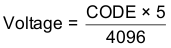
The bipolar analog input conversion values are stored in straight binary format in the ADC-Data registers (address 0x20 – 0x37). The LSB size for these channels is 10 × VREF/4096. With the internal reference equal to 2.5-V the voltage value is given by,
A typical application for the bipolar channels is monitoring of the twelve DAC outputs in the device. In this application the bipolar inputs can be driven directly. However in applications where the signal source has high impedance, it is recommended that the analog input is buffered prior to be input to the AMC7832. When driven from a low impedance source such as the AMC7832 DAC outputs, the network is designed to settle well before the start of conversion. Additional impedance may affect the settling and divider accuracy of this network.
8.3.2.1.2 Unipolar Analog Inputs
In addition to the bipolar input channels, the AMC7832 includes five unipolar analog inputs. The analog input range for these channels is 0-V to 2 × VREF with the LSB size for these channels given by 2 × VREF/4096.
The unipolar analog input conversion values are stored in straight binary format in the ADC-Data registers (address 0x38 – 0x41). With the internal reference equal to 2.5-V the voltage value is given by,
In applications where the signal source has high impedance, it is recommended that the unipolar analog input is buffereded externally.
8.3.2.2 ADC Sequencing
The AMC7832 ADC supports two conversion methods: direct-mode and auto-mode. The conversion method can be selected in the ADC Configuration register (address 0x10). The default conversion method is direct-mode.
In both methods, the single channel or sequence of channels to be converted by the ADC must be first configured in the ADC MUX Configuration registers (address 0x13 – 0x15). The input channels to the ADC include 12 external bipolar inputs, 5 external unipolar inputs and the internal temperature sensor.
In direct-mode conversion, the selected ADC input channels are converted on demand by issuing an ADC trigger signal. After the last enabled channel is converted, the ADC goes into idle state and waits for a new trigger.
In auto-mode conversion, the selected ADC input channels are converted continuously. The conversion cycle is initiated by issuing an ADC trigger. Upon completion of the first conversion sequence another sequence is automatically started. Conversion of the selected channels is done repeatedly until the auto-mode conversion is stopped by issuing a second trigger signal. To ensure data for all channels is updated correctly in the ADC data registers the auto-mode conversion stop trigger should be synchronized with the data available indicator signal (DAV, terminal 12).
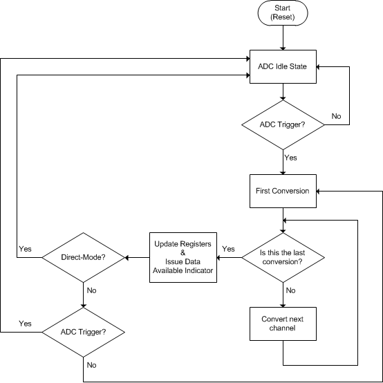 Figure 44. AMC7832 ADC Conversion Sequence
Regardless of the selected conversion method, the following registers should only be updated while the ADC is in idle state:
- ADC Configuration Register (address 0x10)
- False Alarm Configuration Register (address 0x11)
- ADC MUX Configuration Registers (address 0x13 – 0x15)
- Threshold Registers (0x80 – 0x97)
- Hysteresis Register (0xA0 – 0xA5)
- Power Down Registers (0xB2 - 0xB3)
8.3.2.3 ADC Synchronization
A trigger signal is required for getting the ADC in and out of idle state. The ADC trigger can be generated either through software (ICONV bit in the ADC Trigger Register, 0xC0) or hardware (GPIO2/ADCTRIG, terminal 11). In order to use the GPIO2/ADCTRIG terminal as an ADC trigger, the terminal must be configured accordingly in the GPIO Configuration register (address 0x12). When the terminal is configured as a trigger, a falling edge starts the sampling and conversion of the ADC.
The ADC Data registers (0x20 – 0x41) and Temperature Data registers (0x78 – 0x79) should only be accessed while the ADC is in idle state or between conversion sequences if the ADC is in auto-mode. A data available indicator signal is generated by the device to track the ADC status. Failure to satisfy the synchronization requirements could lead to erroneous data reads.
The data available indicator signal is output through the GPIO3/DAV terminal. The GPIO3/DAV terminal must be configured in the GPIO Configuration register (address 0x12) as an interrupt. In addition to the terminal indicator the device provides a data available flag accessible through the serial interface (DAVF bit in the General Status Register, 0x72). The DAV terminal is available in both auto and direct-mode but the DAVF flag is only available in direct mode.
The terminal and flag behavior are dependent on the conversion mode. In direct-mode, after the conversion is completed and the ADC returns to idle state, the DAVF bit is set immediately to ‘1’ and the DAV terminal is active (low) to indicate new data is available. The terminal and flag are cleared automatically once a new conversion is started or one of the ADC Data or Temperature Data registers is accessed. In auto-mode, the DAVF bit is fixed to ‘0’ and therefore synchronization is always done through the DAV terminal. After one auto-mode conversion sequence is complete a 1µs pulse (low) is issued on the DAV terminal. When an auto-mode conversion needs to be stopped it is recommended to do so in synchronization with DAV.
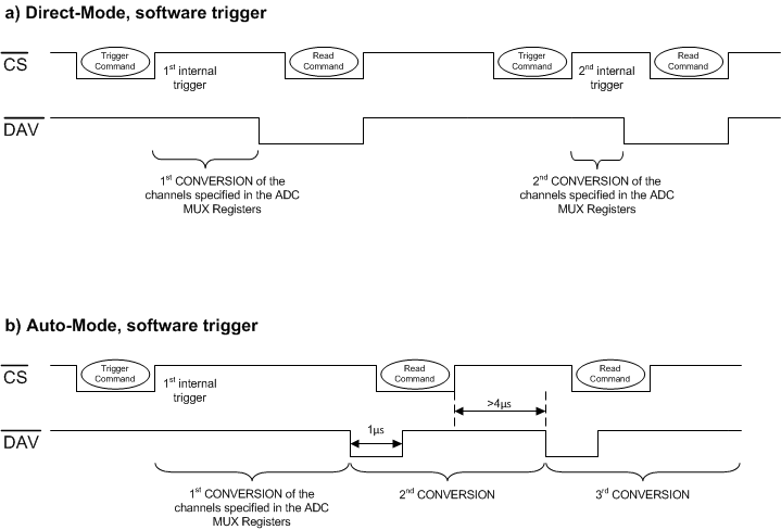 Figure 45. ADC Software Trigger Synchronization
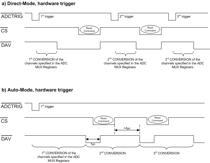
8.3.2.4 Programmable Out-of-Range Alarms
The AMC7832 is capable of continuously analyzing the 5 external unipolar inputs and internal temperature sensor conversion results for normal operation.
Normal operation is established through the Lower and Upper Threshold registers (address 0x80 – 0x97). When any of the monitored inputs is out of the specified range, an alarm event is issued and the global alarm bit, GALR in the General Status register (0x72) is set. Details on the source of the alarm event can be determined through the Alarm Status registers (0x70 – 0x71).
The ALARM-LATCH-DIS bit in the ALARMOUT Source 1 register (address 0x1D) sets the latching behavior for all alarms (except for the ALARMIN alarm which is always unlatched). When the ALARM-LATCH-DIS bit is cleared to ‘0’ the alarm bits in the Alarm Status registers are latched. The alarm bits are referred to as being latched because they remain set until read by software. This design ensures that out-of-limit events cannot be missed if the software is polling the device periodically. The alarm bits are cleared when their corresponding Alarm Status register is read, and are reasserted if the out-of limit condition still exists on the next monitoring cycle, unless otherwise noted. When the ALARM-LATCH-DIS bit is set to ‘1’, the alarm bits are not latched. The alarm bits in the Alarm Status registers go to '0' when the error condition subsides, regardless of whether the bit is read or not.
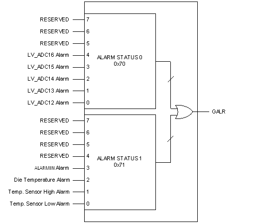 Figure 47. AMC7832 Alarm Status Register
All of the alarms can be set to activate the ALARMOUT terminal. The GPIO1/ALARMOUT terminal must be configured accordingly in the GPIO Configuration register (address 0x12) to enable this functionality. The ALARMOUT terminal works as an interrupt to the host so that it may query the Alarm Status registers to determine the alarm source. Any alarm event can activate the terminal as long as the alarm is not masked in the ALARMOUT Source registers (address 0x1C – 0x1D). When an alarm event is masked, the occurrence of the event sets the corresponding status bit in the Alarm Status registers to '1', but does not activate the ALARMOUT terminal.
8.3.2.4.1 Unipolar Inputs Out-of-Range Alarms
The AMC7832 provides out-of-range detection for the five external unipolar ADC inputs (LV_ADC12 to LV_ADC16, terminals 41 - 45). When the measurement is out-of-range, the corresponding alarm bit in the Alarm Status 0 register (address 0x70) is set to '1' to flag the out-of-range condition. The values in the ADC Upper and Lower Threshold registers (address 0x80 – 0x93) define the upper and lower bound thresholds for all five inputs.
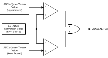 Figure 48. Unipolar Inputs Out-of-Range Alarms
8.3.2.4.2 Internal Temperature Sensor Out-of-Range Alarms
The AMC7832 includes high-limit and low-limit detection for the internal temperature sensor. The values in the LT Upper and Lower Threshold registers (address 0x94 – 0x97) set the limits for the temperature sensor. The temperature sensor detector can issue either a high-alarm (LT-HIGH-ALR bit) or a low-alarm (LT-LOW-ALR bit) in the Alarm Status 1 register (address 0x71) depending on whether the high or low thresholds were exceeded. To implement single, upper-bound threshold detection for the temperature sensor, the host processor can set the upper-bound threshold to the desired value and the lower-bound threshold to the default value. For lower-bound threshold detection, the host processor can set the lower-bound threshold to the desired value and the upper-bound threshold to the default value.
In addition to the programmable threshold alarms the temperature sensor detection circuit also includes a die thermal alarm flag which continuously monitors the die temperature. When the die temperatures exceeds +150˚C the die thermal alarm flag (THERM-ALR bit) in the Alarm Status 1 register (address 0x71) is set. The internal temperature sensor must be enabled for this alarm to be functional.
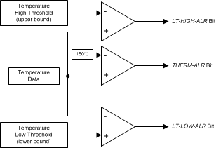 Figure 49. Internal Temperature Out-of-Range Alarms
8.3.2.4.3 ALARMIN Alarm
The AMC7832 offers the option of using an external interrupt signal, such as the output of a comparator as an alarm event. The GPIO0/ALARMIN terminal is used as the alarm input and must be configured accordingly in the GPIO Configuration register (address 0x12). When the terminal is configured as an alarm input it is active low.
A typical application for ALARMIN is to use it as a hardware interrupt responsible for forcing one or more DACs to a clear state: the DAC is loaded with a zero-code input and the output voltage is set accordingly to the operating output range, however the DAC buffer or active registers do not change (refer to the DAC section for more details). To enable this functionality ALARMIN must be enabled as a DAC clear alarm source in the DAC Clear Source 1 register (address 0x1B). Additionally the DAC outputs to be cleared by the ALARMIN terminal need to be specified in the DAC Clear Enable registers (address 0x18 – 0x19).
In this application when the ALARMIN terminal goes low, all the DACs set to clear in response to the ALARMIN alarm in the DAC Clear Enable registers enter a clear state. When the ALARMIN terminal goes back high the DACs get re-loaded with the contents of the DAC active registers thus allowing the DAC outputs to return to their previous operating point without any additional commands.
8.3.2.4.4 Hysteresis
If a monitored signal is out of range and the alarm is enabled, the corresponding alarm bit is set ('1'). However, the alarm condition is cleared only when the conversion result returns to a value of at least HYST below the value of the high threshold register, or HYST above the value of the low threshold register. The ADC and LT Hysteresis registers (address 0xA0 – 0xA4) store the hys value for the external unipolar inputs and internal temperature sensor programmable alarms. HYST is the programmable value of hysteresis: 0 LSB to 127 LSB for the unipolar inputs alarms, and 0°C to +31°C for the internal temperature sensor alarms. The die thermal alarm hysteresis is fixed at 8°C.
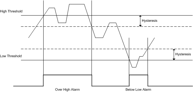 Figure 50. AMC7832 Hysteresis
8.3.2.4.5 False-Alarm Protection
In order to prevent false alarms an alarm event is only registered when the monitored signal is out of range for an N number of consecutive conversions. If the monitored signal returns to the normal range before N consecutive conversions, an alarm event is not issued. The false alarm factor N for the unipolar input and local temperature sensor out-of-range alarms can be configured in the False Alarm Configuration register (address 0x11).
8.3.3 Internal Temperature Sensor
The AMC7832 has an on-chip temperature sensor used to measure the device die temperature. The normal operating temperature range for the internal temperature sensor is limited by the operating temperature range of the device (–40°C to +125°C).
The temperature sensor results are converted by the device ADC at a lower speed than the analog input channels. Temperature can be monitored either continuously or as a single-time conversion depending on whether the ADC is configured in Auto mode or Direct mode (refer to the ADC section for more details). If the temperature sensor is not needed, it can be disabled in the ADC MUX Configuration 2 register (address 0x15). By default the temperature sensor is disabled and not converted by the ADC.
The temperature sensor gives 0.25°C resolution over the operating temperature range. The temperature value is stored in 12-bit two’s complement format in the Temperature data registers (address 0x78 – 0x79).
Table 3. Temperature Sensor Data Format
| TEMPERATURE (°C) | DIGITAL CODE |
|---|---|
| -40 | 1111 0110 0000 |
| -25 | 1111 1001 1100 |
| -10 | 1111 1101 1000 |
| -0.25 | 1111 1111 1111 |
| 0 | 0000 0000 0000 |
| +0.25 | 0000 0000 0001 |
| +10 | 0000 0010 1000 |
| +25 | 0000 0110 0100 |
| +50 | 0000 1100 1000 |
| +75 | 0001 0010 1100 |
| +100 | 0001 1001 0000 |
| +105 | 0001 1010 0100 |
| +125 | 0001 1111 0100 |
If the output data MSB is ‘0’, the temperature can be calculated by,


8.3.4 Internal Reference
The AMC7832 includes a high performance internal reference for the on-chip ADC and twelve DACs. The internal reference is a 2.5-V bipolar transistor-based, precision bandgap reference. A compensation capacitor (4.7-μF, typical) should be connected between the REF_CMP terminal and AGND2.
The AMC7832 includes two buffers to access the internal reference voltage through terminals REF_OUT1 and REF_OUT2. If unused, the two reference buffers can be powered down independently in the Power-down 1 register (address 0xB3). A third buffer is used to drive the ADC and should not be used to drive any external circuitry. The ADC reference buffer is powered down by default and should be enabled in the ADC Configuration Register (address 0x10) during device initialization.
The REF_OUT1 and REF_OUT2 outputs can directly drive the VRANGEA,B,C,D inputs thus enabling adjustment of the DAC output ranges without the need for external circuitry. The internal reference buffers are not intended to drive external loads. If driving an external load, a high impedance buffer amplifier is required.
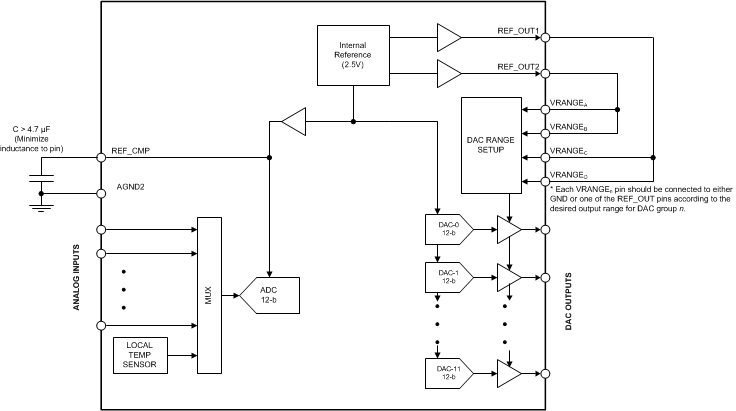 Figure 51. AMC7832 Internal Reference
 8.3.5 General Purpose I/Os
The AMC7832 includes eight General Purpose I/O (GPIO) terminals, each with an internal 48-kΩ pull-up resistor to IOVDD. The GPIO[0-3] terminals have dual functionality and can be programmed as either bidirectional digital I/O terminals or interrupt signals in the GPIO Configuration register (address 0x12). The GPIO[4-7] terminals are dedicated GPIOs.
Table 4. Dual Functionality GPIO Pins
| PIN | DEFAULT PIN NAME | ALTERNATIVE PIN NAME | ALTERNATIVE FUNCTIONALITY |
|---|---|---|---|
| 9 | GPIO0 | ALARMIN | DAC clear control signal. |
| 10 | GPIO1 | ALARMOUT | Global alarm output. |
| 11 | GPIO2 | ADCTRIG | External ADC conversion trigger. |
| 12 | GPIO3 | DAV | ADC data available indicator. |
The GPIOs can receive an input or produce an output. When the GPIO acts as an output its status is determined by the corresponding GPIO bit in the GPIO Register (address 0x7A).
To use a GPIO terminal as an input, the corresponding GPIO bit in the GPIO Register must be set to '1'. When a GPIO terminal acts as input, the digital value on the terminal is acquired by reading the corresponding GPIO bit. After a power-on reset or any forced reset, all GPIO bits are set to '1', and the GPIO terminals have a 48-kΩ input impedance to IOVDD.
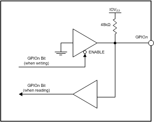 Figure 52. AMC7832 GPIO Pin
8.4 Programming
The AMC7832 is controlled through a flexible four-wire serial interface that is compatible with SPI type interfaces used on many microcontrollers and DSP controllers. The interface provides read/write access to all registers of the AMC7832.
Each serial interface access cycle is exactly (N+2) bytes long, where N is the number of data bytes. A frame is initiated by asserting CS low. The frame ends when CS is deasserted high. In MSB first mode, the first bit transferred is the R/W bit. The next 15 bits are the register address (32768 addressable registers), and the remaining bits are data. For all writes, data is committed in bytes as the 8th data bit of a data field is clocked in on the rising edge of SCLK. If the write access is not a multiple of 8 clocks, the trailing data bits will not be committed. On read access, data is clocked out on the falling edge of SCLK on the SDO terminal.
The figures below show the access protocol used by the interface. Data is by default accepted as MSB (Most Significant Bit) first but the AMC7832 can be configured to accept LSB (Least Significant Bit) first operations as long as the LSB_Order bit in the Interface Configuration 0 register (address 0x00) is set accordingly.
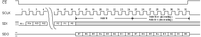 Figure 53. Serial Interface Write Bus Cycle
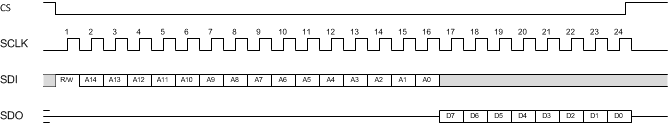 Figure 54. Serial Interface Read Bus Cycle
For operations that require large amounts of data to be passed to or from the AMC7832, streaming mode is supported. In streaming mode multiple bytes of data can be written to or read from the AMC7832 without specifically providing instructions for each byte and is implemented by continually holding the CS active and continuing to shift new data in or old data out of the device.
The instruction phase includes the starting address. The AMC7832 starts reading or writing data to this address and continues as long as CS is asserted and single byte writes has not been enabled in the Interface Configuration 1 register (address 0x01). The AMC7832 automatically increments or decrements the address depending on the setting of the address ascension bit in the Interface Configuration 0 register (address 0x00).
If the address is decrementing and 0x0000 is reached, the next address used is address 0x7FFF. If the address is incrementing and address 0x7FFF is reached, the next address used is 0x0000. Care should be taken when writing to 0x0000 and 0x0001 as writing to these addresses may change the configuration of the serial interface. Therefore it is advised that 0x0001 be the first address written and that streaming stops prior to reaching this address.
The figures below show the access protocol used in streaming mode.
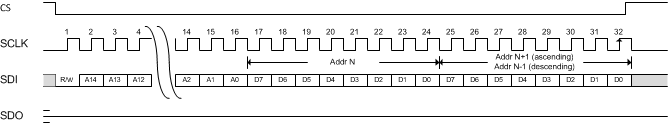 Figure 55. Serial Interface Streaming Write Example
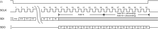 Figure 56. Serial Interface Streaming Read Example
8.5 Register Map
Table 5. Register Map
| ADDRESS (HEX) |
R/W | DEFAULT (HEX) |
REGISTER | ADDRESS (HEX) |
R/W | DEFAULT (HEX) |
REGISTER | |
|---|---|---|---|---|---|---|---|---|
| 0x00 | R/W | 3C | Interface Configuration 0 | 0x54 | R/W | 00 | DACA10-Data (low byte) | |
| 0x01 | R/W | 00 | Interface Configuration 1 | 0x55 | R/W | 00 | DACA10-Data (high byte) | |
| 0x02 | R/W | 03 | Device Configuration | 0x56 | R/W | 00 | DACA11-Data (low byte) | |
| 0x03 | R | 08 | Chip Type | 0x57 | R/W | 00 | DACA11-Data (high byte) | |
| 0x04 | R | 32 | Chip ID (low byte) | 0x58 | R/W | 00 | DACB6-Data (low byte) | |
| 0x05 | R | 0C | Chip ID (high byte) | 0x59 | R/W | 00 | DACB6-Data (high byte) | |
| 0x06 | R | 00 | Chip Version | 0x5A | R/W | 00 | DACB7-Data (low byte) | |
| 0x07 – 0x0B | — | — | Reserved | 0x5B | R/W | 00 | DACB7-Data (high byte) | |
| 0x0C | R | 51 | Manufacturer ID (low byte) | 0x5C | R/W | 00 | DACC0-Data (low byte) | |
| 0x0D | R | 04 | Manufacturer ID (high byte) | 0x5D | R/W | 00 | DACC0-Data (high byte) | |
| 0x0E | — | — | Reserved | 0x5E | R/W | 00 | DACC1-Data (low byte) | |
| 0x0F | W | 00 | Register Update | 0x5F | R/W | 00 | DACC1-Data (high byte) | |
| 0x10 | R/W | 00 | ADC Configuration | 0x60 | R/W | 00 | DACD2-Data (low byte) | |
| 0x11 | R/W | 07 | False Alarm Configuration | 0x61 | R/W | 00 | DACD2-Data (high byte) | |
| 0x12 | R/W | 00 | GPIO Configuration | 0x62 | R/W | 00 | DACD3-Data (low byte) | |
| 0x13 | R/W | 00 | ADC MUX Configuration 0 | 0x63 | R/W | 00 | DACD3-Data (high byte) | |
| 0x14 | R/W | 00 | ADC MUX Configuration 1 | 0x64 | R/W | 00 | DACD4-Data (low byte) | |
| 0x15 | R/W | 00 | ADC MUX Configuration 2 | 0x65 | R/W | 00 | DACD4-Data (high byte) | |
| 0x16 | — | — | Reserved | 0x66 | R/W | 00 | DACD5-Data (low byte) | |
| 0x17 | — | — | Reserved | 0x67 | R/W | 00 | DACD5-Data (high byte) | |
| 0x18 | R/W | 00 | DAC Clear Enable 0 | 0x68–0x6F | — | — | Reserved | |
| 0x19 | R/W | 00 | DAC Clear Enable 1 | 0x70 | R | 00 | Alarm Status 0 | |
| 0x1A | R/W | 00 | DAC Clear Source 0 | 0x71 | R | 00 | Alarm Status 1 | |
| 0x1B | R/W | 00 | DAC Clear Source 1 | 0x72 | R | 00 | General Status | |
| 0x1C | R/W | 00 | ALARMOUT Source 0 | 0x73–0x77 | R/W | 00 | Reserved | |
| 0x1D | R/W | 00 | ALARMOUT Source 1 | 0x78 | R | 00 | Temperature Data (low byte) | |
| 0x1E | R/W | 00 | DAC Range | 0x79 | R | 00 | Temperature Data (high byte) | |
| 0x1F | — | — | Reserved | 0x7A | R/W | FF | GPIO | |
| 0x20 | R | 00 | ADC0-Data (low byte) | 0x7B–0x7F | — | — | Reserved | |
| 0x21 | R | 00 | ADC0-Data (high byte) | 0x80 | R/W | FF | ADC12-Upper-Thresh (low byte) | |
| 0x22 | R | 00 | ADC1-Data (low byte) | 0x81 | R/W | 0F | ADC12-Upper-Thresh (high byte) | |
| 0x23 | R | 00 | ADC1-Data (high byte) | 0x82 | R/W | 00 | ADC12-Lower-Thresh (low byte) | |
| 0x24 | R | 00 | ADC2-Data (low byte) | 0x83 | R/W | 00 | ADC12-Lower-Thresh (high byte) | |
| 0x25 | R | 00 | ADC2-Data (high byte) | 0x84 | R/W | FF | ADC13-Upper-Thresh (low byte) | |
| 0x26 | R | 00 | ADC3-Data (low byte) | 0x85 | R/W | 0F | ADC13-Upper-Thresh (high byte) | |
| 0x27 | R | 00 | ADC3-Data (high byte) | 0x86 | R/W | 00 | ADC13-Lower-Thresh (low byte) | |
| 0x28 | R | 00 | ADC4-Data (low byte) | 0x87 | R/W | 00 | ADC13-Lower-Thresh (high byte) | |
| 0x29 | R | 00 | ADC4-Data (high byte) | 0x88 | R/W | FF | ADC14-Upper-Thresh (low byte) | |
| 0x2A | R | 00 | ADC5-Data (low byte) | 0x89 | R/W | 0F | ADC14-Upper-Thresh (high byte) | |
| 0x2B | R | 00 | ADC5-Data (high byte) | 0x8A | R/W | 00 | ADC14-Lower-Thresh (low byte) | |
| 0x2C | R | 00 | ADC6-Data (low byte) | 0x8B | R/W | 00 | ADC14-Lower-Thresh (high byte) | |
| 0x2D | R | 00 | ADC6-Data (high byte) | 0x8C | R/W | FF | ADC15-Upper-Thresh (low byte) | |
| 0x2E | R | 00 | ADC7-Data (low byte) | 0x8D | R/W | 0F | ADC15-Upper-Thresh (high byte) | |
| 0x2F | R | 00 | ADC7-Data (high byte) | 0x8E | R/W | 00 | ADC15-Lower-Thresh (low byte) | |
| 0x30 | R | 00 | ADC8-Data (low byte) | 0x8F | R/W | 00 | ADC15-Lower-Thresh (high byte) | |
| 0x31 | R | 00 | ADC8-Data (high byte) | 0x90 | R/W | FF | ADC16-Upper-Thresh (low byte) | |
| 0x32 | R | 00 | ADC9-Data (low byte) | 0x91 | R/W | 0F | ADC16-Upper-Thresh (high byte) | |
| 0x33 | R | 00 | ADC9-Data (high byte) | 0x92 | R/W | 00 | ADC16-Lower-Thresh (low byte) | |
| 0x34 | R | 00 | ADC10-Data (low byte) | 0x93 | R/W | 00 | ADC16-Lower-Thresh (high byte) | |
| 0x35 | R | 00 | ADC10-Data (high byte) | 0x94 | R/W | FF | LT-Upper-Thresh (low byte) | |
| 0x36 | R | 00 | ADC11-Data (low byte) | 0x95 | R/W | 07 | LT-Upper-Thresh (high byte) | |
| 0x37 | R | 00 | ADC11-Data (high byte) | 0x96 | R/W | 00 | LT-Lower-Thresh (low byte) | |
| 0x38 | R | 00 | ADC12-Data (low byte) | 0x97 | R/W | 08 | LT-Lower-Thresh (high byte) | |
| 0x39 | R | 00 | ADC12-Data (high byte) | 0x98–0x9F | — | — | Reserved | |
| 0x3A | R | 00 | ADC13-Data (low byte) | 0xA0 | R/W | 08 | ADC12-Hysteresis | |
| 0x3B | R | 00 | ADC13-Data (high byte) | 0xA1 | R/W | 08 | ADC13-Hysteresis | |
| 0x3C | R | 00 | ADC14-Data (low byte) | 0xA2 | R/W | 08 | ADC14-Hysteresis | |
| 0x3D | R | 00 | ADC14-Data (high byte) | 0xA3 | R/W | 08 | ADC15-Hysteresis | |
| 0x3E | R | 00 | ADC15-Data (low byte) | 0xA4 | R/W | 08 | ADC16-Hysteresis | |
| 0x3F | R | 00 | ADC15-Data (high byte) | 0xA5 | R/W | 08 | LT-Hysteresis | |
| 0x40 | R | 00 | ADC16-Data (low byte) | 0xA6—0xAF | — | — | Reserved | |
| 0x41 | R | 00 | ADC16-Data (high byte) | 0xB0 | R/W | 00 | DAC Clear 0 | |
| 0x42–0x4F | — | — | Reserved | 0xB1 | R/W | 00 | DAC Clear 1 | |
| 0x50 | R/W | 00 | DACA8-Data (low byte) | 0xB2 | R | 00 | Power-Down 0 | |
| 0x51 | R/W | 00 | DACA8-Data (high byte) | 0xB3 | R/W | 00 | Power-Down 1 | |
| 0x52 | R/W | 00 | DACA9-Data (low byte) | 0xB4–0xBF | — | — | Reserved | |
| 0x53 | R/W | 00 | DACA9-Data (high byte) | 0xC0 | W | 00 | ADC Trigger |
8.5.1 Interface Configuration: Address 0x00 – 0x02
Table 6. Register name: Interface Configuration 0 – Address: 0x00, Default: 0x3C (READ/WRITE)
| REGISTER NAME |
ADDRESS | BIT | NAME | DESCRIPTION | DEFAULT VALUE |
|---|---|---|---|---|---|
| Interface Config 0 |
0x00 | 7 | SOFT-RESET | Soft reset (self-clearing) 0: no action 1: reset – resets everything except address 0x00, 0x01 |
0 |
| 6 | LSB-ORDER | LSB First 0: MSB first 1: LSB first |
0 | ||
| 5 | ADDR-ASCEND | Address Ascend 0: Descend – decrements address while streaming (address wrap from 0x0000 to 0x7FFF) 1: Ascend – increments address while streaming (address wrap from 0x7FFF to 0x0000) |
1 | ||
| 4 | Reserved | Reserved for factory use | 1 | ||
| 3:0 | REVERSE-CONFIG | Bits 3:0 should always mirror bits 7:4 so that it does not matter whether the part is in MSB or LSB first mode. Bits should be set as follows: Bit 0 = Bit 7 Bit 1 = Bit 6 Bit 2 = Bit 5 Bit 3 = Bit 4 |
0xC |
Table 7. Register name: Interface Configuration 1 – Address: 0x01, Default: 0x00 (READ/WRITE)
| REGISTER NAME |
ADDRESS | BIT | NAME | DESCRIPTION | DEFAULT VALUE |
|---|---|---|---|---|---|
| Interface Config 1 | 0x01 | 7 | SINGLE-INSTR | Single instruction enable 0: streaming mode (default) 1: single instruction |
0 |
| 6 | Reserved | Reserved for factory use | 0 | ||
| 5 | READBACK | Read back 0: DAC read back from active registers (default) 1: DAC read back from buffer registers |
0 | ||
| 4 | Reserved | Reserved for factory use | 0 | ||
| 3 | Reserved | Reserved for factory use | 0 | ||
| 2 | Reserved | Reserved for factory use | 0 | ||
| 1 | Reserved | Reserved for factory use | 0 | ||
| 0 | Reserved | Reserved for factory use | 0 |
Table 8. Register name: Device Configuration – Address: 0x02, Default: 0x03 (READ/WRITE)
| REGISTER NAME |
ADDRESS | BIT | NAME | DESCRIPTION | DEFAULT VALUE |
|---|---|---|---|---|---|
| Device Config | 0x02 | 7:2 | Reserved | Reserved for factory use | All zeros |
| 1:0 | POWER-MODE | Mode: 00: Normal operation – full power and full performance 11: Sleep – lowest power, non-operational except SPI One time overwrite of the power-down registers (0xB2 and 0xB3) |
11 |
8.5.2 Device Identification: Address 0x03 – 0x0D
Table 9. Register name: Chip Type – Address: 0x03, Default: 0x08 (READ ONLY)
| REGISTER NAME |
ADDRESS | BIT | NAME | DESCRIPTION | DEFAULT VALUE |
|---|---|---|---|---|---|
| Chip Type | 0x03 | 7:4 | Reserved | Reserved for factory use | 0x0 |
| 3:0 | CHIP-TYPE | Identifies the device as a precision analog monitor and control | 0x8 |
Table 10. Register name: Chip ID low byte – Address: 0x04, Default: 0x32 (READ ONLY)
| REGISTER NAME |
ADDRESS | BIT | NAME | DESCRIPTION | DEFAULT VALUE |
|---|---|---|---|---|---|
| Chip ID Low Byte | 0x04 | 7:0 | CHIPID-LOW | Chip ID. Low byte | 0x32 |
Table 11. Register name: Chip ID high byte – Address: 0x05, Default: 0x0C (READ ONLY)
| REGISTER NAME |
ADDRESS | BIT | NAME | DESCRIPTION | DEFAULT VALUE |
|---|---|---|---|---|---|
| Chip ID High Byte | 0x05 | 7:0 | CHIPID-HIGH | Chip ID. High byte | 0x0C |
Table 12. Register name: Version ID – Address: 0x06, Default: 0x00 (READ ONLY)
| REGISTER NAME |
ADDRESS | BIT | NAME | DESCRIPTION | DEFAULT VALUE |
|---|---|---|---|---|---|
| Version ID | 0x06 | 7:0 | VERSIONID | AMC7832 Version ID. Subject to change. | 0x00 |
Table 13. Register name: Manufacturer ID low byte – Address: 0x0C, Default: 0x51 (READ ONLY)
| REGISTER NAME |
ADDRESS | BIT | NAME | DESCRIPTION | DEFAULT VALUE |
|---|---|---|---|---|---|
| Manuf. ID Low Byte | 0x0C | 7:0 | VENDORID-LOW | Manufacturer ID. Low byte | 0x51 |
Table 14. Register name: Manufacturer ID high byte – Address: 0x0D, Default: 0x04 (READ ONLY)
| REGISTER NAME |
ADDRESS | BIT | NAME | DESCRIPTION | DEFAULT VALUE |
|---|---|---|---|---|---|
| Manuf. ID High Byte | 0x0D | 7:0 | VENDORID-HIGH | Manufacturer ID. High byte | 0x04 |
8.5.3 Register Update (Buffered Registers): Address 0x0F
Table 15. Register name: Register Update – Address: 0x0F, Default: 0x00 (SELF CLEARING)
| REGISTER NAME |
ADDRESS | BIT | NAME | DESCRIPTION | DEFAULT VALUE |
|---|---|---|---|---|---|
| Register Update | 0x0F | 7:1 | Reserved | Reserved for factory use | All zeros |
| 0 | UPDATE | Update (self clearing) 0: disabled 1: enabled – transfers data from buffers to active registers (DAC registers only) |
0 |
8.5.4 General Device Configuration: Address 0x10 – 0x17
Table 16. Register name: ADC Configuration – Address: 0x10, Default: 0x00 (READ/WRITE)
| REGISTER NAME |
ADDRESS | BIT | NAME | DESCRIPTION | DEFAULT VALUE |
|---|---|---|---|---|---|
| ADC Config | 0x10 | 7 | CMODE | ADC Conversion Mode Bit. This bit selects the ADC conversion mode. 0: Direct mode. The analog inputs specified in the ADC channel registers are converted sequentially one time. When one set of conversions is complete, the ADC is idle and waits for a new trigger. 1: Auto mode. The analog inputs specified in the AMC channel registers are converted sequentially and repeatedly. When one set of conversions is complete, the ADC multiplexer returns to the first channel and repeats the process. In this mode data should be read synchronously with the DAV terminal. |
0 |
| 6:5 | CONV-RATE[1:0] | ADC Conversion rate bits | 00 | ||
| 4 | ADC-REF-BUFF | ADC Reference Buffer bit. This bit must be set to 1 after device power-up to enable the internal reference buffer driving the ADC. 0: ADC reference buffer is disabled. 1: ADC reference buffer is enabled. |
0 | ||
| 3:0 | Reserved | Reserved for factory use | 0000 |
Table 17. Register name: False Alarm Configuration – Address: 0x11, Default: 0x70 (READ/WRITE)
| REGISTER NAME |
ADDRESS | BIT | NAME | DESCRIPTION | DEFAULT VALUE |
|||
|---|---|---|---|---|---|---|---|---|
| False Alarm Config | 0x10 | 7:5 | CH-FALR-CT[2:0] | False alarm protection for ADC channels. | 011 | |||
| CH-FALR-CT | N CONSECUTIVE SAMPLES BEFORE ALARM IS SET | |||||||
| 000 | 1 | |||||||
| 001 | 4 | |||||||
| 010 | 8 | |||||||
| 011 | 16 (default) | |||||||
| 100 | 32 | |||||||
| 101 | 64 | |||||||
| 110 | 128 | |||||||
| 111 | 256 | |||||||
| 4:3 | TEMP-FALR-CT[1:0] | False alarm protection for temperature sensor. | 10 | |||||
| TEMP-FALR-CT | N CONSECUTIVE SAMPLES BEFORE ALARM IS SET | |||||||
| 00 | 1 | |||||||
| 01 | 2 | |||||||
| 10 | 4 (default) | |||||||
| 11 | 8 | |||||||
| 2:0 | Reserved | Reserved for factory use | 000 | |||||
Table 18. Register name: GPIO Configuration – Address: 0x12, Default: 0x00 (READ/WRITE)
| REGISTER NAME |
ADDRESS | BIT | NAME | DESCRIPTION | DEFAULT VALUE |
|---|---|---|---|---|---|
| GPIO Config | 0x12 | 7:5 | Reserved | Reserved for factory use | 000 |
| 4 | Reserved | Reserved for factory use | 0 | ||
| 3 | EN-DAV | DAV terminal enable 0: GPIO3 operation (default) 1: DAV operation |
0 | ||
| 2 | EN-ADCTRIG | ADCTRIG terminal enable 0: GPIO2 operation (default) 1: ADCTRIG operation |
0 | ||
| 1 | EN-ALARMOUT | ALARMOUT terminal enable 0: GPIO1 operation (default) 1: ALARMOUT operation |
0 | ||
| 0 | EN-ALARMIN | ALARMIN terminal enable 0: GPIO0 operation (default) 1: ALARMIN operation |
0 |
Table 19. Register name: ADC MUX Configuration 0 – Address: 0x13, Default: 0x00 (READ/WRITE)
| REGISTER NAME |
ADDRESS | BIT | NAME | DESCRIPTION | DEFAULT VALUE |
|---|---|---|---|---|---|
| ADC MUX Config 0 | 0x13 | 7 | CH7 | When set to ‘1’ the corresponding analog input channel ADC_n is accessed during an ADC conversion cycle. When cleared to ‘0’ the corresponding input channel ADC_n is ignored during an ADC conversion cycle. |
0 |
| 6 | CH6 | 0 | |||
| 5 | CH5 | 0 | |||
| 4 | CH4 | 0 | |||
| 3 | CH3 | 0 | |||
| 2 | CH2 | 0 | |||
| 1 | CH1 | 0 | |||
| 0 | CH0 | 0 |
Table 20. Register name: ADC MUX Configuration 1 – Address: 0x14, Default: 0x00 (READ/WRITE)
| REGISTER NAME |
ADDRESS | BIT | NAME | DESCRIPTION | DEFAULT VALUE |
|---|---|---|---|---|---|
| ADC MUX Config 1 | 0x14 | 7 | CH15 | When set to ‘1’ the corresponding analog input channel ADC_n is accessed during an ADC conversion cycle. When cleared to ‘0’ the corresponding input channel ADC_n is ignored during an ADC conversion cycle. |
0 |
| 6 | CH14 | 0 | |||
| 5 | CH13 | 0 | |||
| 4 | CH12 | 0 | |||
| 3 | CH11 | 0 | |||
| 2 | CH10 | 0 | |||
| 1 | CH9 | 0 | |||
| 0 | CH8 | 0 |
Table 21. Register name: ADC MUX Configuration 2 – Address: 0x15, Default: 0x00 (READ/WRITE)
| REGISTER NAME |
ADDRESS | BIT | NAME | DESCRIPTION | DEFAULT VALUE |
|---|---|---|---|---|---|
| ADC MUX Config 2 | 0X15 | 7:2 | Reserved | Reserved for factory use | All zeros |
| 1 | TEMP-CH | When set to ‘1’ the local temperature sensor is enabled for ADC conversion. When cleared to ‘0’ the local temperature sensor is ignored. |
0 | ||
| 0 | CH16 | When set to ‘1’ the corresponding analog input channel ADC_n is accessed during an ADC conversion cycle. When cleared to ‘0’ the corresponding input channel ADC_n is ignored during an ADC conversion cycle. |
0 |
Table 22. Register name: DAC Clear Enable 0 – Address: 0x18, Default: 0x00 (READ/WRITE)
| REGISTER NAME |
ADDRESS | BIT | NAME | DESCRIPTION | DEFAULT VALUE |
|---|---|---|---|---|---|
| DAC Clear Enable 0 | 0x18 | 7 | CLREN-C1 | This register determines which DACs go into clear state when a clear event is detected as configured in the DAC-CLEAR-SOURCE registers. If CLRENn = '1', DAC_n is forced into a clear state with a clear event. If CLRENn = '0', a clear event does not affect the state of DAC_n. |
0 |
| 6 | CLREN-C0 | 0 | |||
| 5 | CLREN-B7 | 0 | |||
| 4 | CLREN-B6 | 0 | |||
| 3 | CLREN-A11 | 0 | |||
| 2 | CLREN-A10 | 0 | |||
| 1 | CLREN-A9 | 0 | |||
| 0 | CLREN-A8 | 0 |
Table 23. Register name: DAC Clear Enable 1 – Address: 0x19, Default: 0x00 (READ/WRITE)
| REGISTER NAME |
ADDRESS | BIT | NAME | DESCRIPTION | DEFAULT VALUE |
|---|---|---|---|---|---|
| DAC Clear Enable 1 | 0x19 | 7:4 | Reserved | Reserved for factory use | All zeros |
| 3 | CLREN-D5 | This register determines which DACs go into clear state when a clear event is detected as configured in the DAC-CLEAR-SOURCE registers. If CLRENn = '1', DAC_n is forced into a clear state with a clear event. If CLRENn = '0', a clear event does not affect the state of DAC_n. |
0 | ||
| 2 | CLREN-D4 | 0 | |||
| 1 | CLREN-D3 | 0 | |||
| 0 | CLREN-D2 | 0 |
8.5.5 DAC Clear And ALARMOUT Source Select: Address 0x1A – 0x1D
Table 24. Register name: Register name: DAC Clear Source 0 – Address: 0x1A, Default: 0x00 (READ/WRITE)
| REGISTER NAME |
ADDRESS | BIT | NAME | DESCRIPTION | DEFAULT VALUE |
|---|---|---|---|---|---|
| DAC Clear Source 0 | 0x1A | 7:5 | Reserved | Reserved for factory use | 000 |
| 4 | ADC16-ALR-CLR | This register selects which alarm forces DACs into a clear state, regardless of which DAC operation mode is active, auto or manual. In order for DAC_n to go into clear mode, it must be enabled in the DAC Clear Enable registers. | 0 | ||
| 3 | ADC15-ALR-CLR | 0 | |||
| 2 | ADC14-ALR-CLR | 0 | |||
| 1 | ADC13-ALR-CLR | 0 | |||
| 0 | ADC12-ALR-CLR | 0 |
Table 25. Register name: Register name: DAC Clear Source 1 – Address: 0x1B, Default: 0x00 (READ/WRITE)
| REGISTER NAME |
ADDRESS | BIT | NAME | DESCRIPTION | DEFAULT VALUE |
|---|---|---|---|---|---|
| DAC Clear Source 1 | 0x1B | 7:4 | Reserved | Reserved for factory use | 0000 |
| 3 | ALARMIN-ALR | This register selects which alarm forces DACs into a clear state, regardless of which DAC operation mode is active, auto or manual. In order for DAC_n to go into clear mode, it must be enabled in the DAC Clear Enable registers. | 0 | ||
| 2 | THERM-ALR | 0 | |||
| 1 | LT-HIGH-ALR | 0 | |||
| 0 | LT-LOW-ALR | 0 |
Table 26. Register name: ALARMOUT Source 0 – Address: 0x1C, Default: 0x00 (READ/WRITE)
| REGISTER NAME |
ADDRESS | BIT | NAME | DESCRIPTION | DEFAULT VALUE |
|---|---|---|---|---|---|
| ALARM OUT Source 0 | 0x1C | 7:5 | Reserved | Reserved for factory use | 000 |
| 4 | ADC16-ALR-OUT | This register selects which alarms can activate the ALARMOUT terminal. The ALARMOUT must be enabled for this function to take effect. | 0 | ||
| 3 | ADC15-ALR-OUT | 0 | |||
| 2 | ADC14-ALR-OUT | 0 | |||
| 1 | ADC13-ALR-OUT | 0 | |||
| 0 | ADC12-ALR-OUT | 0 |
Table 27. Register name: ALARMOUT Source 1 – Address: 0x1D, Default: 0x00 (READ/WRITE)
| REGISTER NAME |
ADDRESS | BIT | NAME | DESCRIPTION | DEFAULT VALUE |
|---|---|---|---|---|---|
| ALARM OUT Source 1 | 0x1D | 7:5 | Reserved | Reserved for factory use | 000 |
| 4 | ALARM-LATCH-DIS | Alarm latch disable bit. When cleared to 0 the alarm bits are latched. When an alarm occurs, the corresponding alarm bit is set to “1”. The alarm bit remains until the error condition subsides and the alarm register is read. Before reading, the alarm bit is not cleared even if the alarm condition disappears. When set to 1 the alarm bits are not latched. When the alarm condition subsides, the alarm bits are cleared regardless of whether the alarm bits have been read or not. | 0 | ||
| 3 | ALRIN-ALR-OUT | This register selects which alarms can activate the ALARMOUT terminal. The ALARMOUT must be enabled for this function to take effect. | 0 | ||
| 2 | THERM-ALR-OUT | 0 | |||
| 1 | LT-HIGH-ALR-OUT | 0 | |||
| 0 | LT-LOW-ALR-OUT | 0 |
8.5.6 DAC Range: Address 0x1E
Table 28. Register name: DAC Range – Address: 0x1E, Default: 0x00 (READ/WRITE)
| REGISTER NAME |
ADDRESS | BIT | NAME | DESCRIPTION | DEFAULT VALUE |
|---|---|---|---|---|---|
| DAC Range | 0xE1 | 7:4 | Reserved | Reserved for factory use | 0000 |
| 3 | DAC-5VRANGED | DAC_n output voltage range bit. VRANGEn terminal is connected to AGND: When the DAC-5VRANGEn bit is cleared to 0 the DAC_n group output voltage range is set to 0-10V. When the DACn-RANGE bit is set to 1 the DAC_n group output voltage range is set to 0-5V. VRANGEn terminal is connected to +2.5V: If the VRANGEn terminal is connected to +2.5V the DAC-5VRANGEn bit must be cleared to 0. |
0 | ||
| 2 | DAC-5VRANGEC | 0 | |||
| 1 | DAC-5VRANGEB | 0 | |||
| 0 | DAC-5VRANGEA | 0 |
8.5.7 ADC Data: Address 0x20 – 0x41
Table 29. Register name: ADCn-Data (low byte) – Address: 0x20 - 0x41, Default: 0x00 (READ ONLY)
| REGISTER NAME |
ADDRESS | BIT | NAME | DESCRIPTION | DEFAULT VALUE |
|---|---|---|---|---|---|
| ADCn Data (low) | 0x20 to 0x41 | 7:0 | ADCn-DATA(7:0) | Stores the 12-bit ADC_n conversion results in straight binary format for both types of inputs channels (unipolar and bipolar) | All zeros |
Table 30. Register name: ADCn-Data (high byte) – Address: 0x20 - 0x41, Default: 0x00 (READ ONLY)
| REGISTER NAME |
ADDRESS | BIT | NAME | DESCRIPTION | DEFAULT VALUE |
|---|---|---|---|---|---|
| ADCn Data (high) | 0x20 to 0x41 | 7:4 | Reserved | Reserved for factory use | All zeros |
| 3:0 | ADCn-DATA (11:8) | Stores the 12-bit ADC_n conversion results in straight binary format for both types of inputs channels (unipolar and bipolar). | All zeros |
8.5.8 DAC Data: Address 0x50 – 0x67
Table 31. Register name: DACn-Data (low byte) – Address: 0x50 - 0x67, Default: 0x00 (READ/WRITE)
| REGISTER NAME |
ADDRESS | BIT | NAME | DESCRIPTION | DEFAULT VALUE |
|---|---|---|---|---|---|
| DACn Data (low) | 0x50 to 0x67 | 7:0 | DACn-DATA(7:0) | Stores the 12-bit data to be loaded to the DAC_n latches in straight binary format. The straight binary format is used for both DAC ranges: -10 to 0V and 0 to 10V. | All zeros |
Table 32. Register name: DACn-Data (high byte) – Address: 0x50 - 0x67, Default: 0x00 (READ/WRITE)
| REGISTER NAME |
ADDRESS | BIT | NAME | DESCRIPTION | DEFAULT VALUE |
|---|---|---|---|---|---|
| DACn Data (high) | 0x50 to 0x67 | 7:4 | Reserved | Reserved for factory use | All zeros |
| 3:0 | DACn-DATA (11:8) | Stores the 12-bit data to be loaded to the DAC_n latches in straight binary format. The straight binary format is used for both DAC ranges: -10 to 0V and 0 to 10V. | All zeros |
8.5.9 Status Registers: Address 0x70 – 0x72
The AMC7832 continuously monitors all unipolar analog inputs and local temperature sensor during normal operation. When any input is out of the specified range N consecutive times, the corresponding alarm bit is set ('1'). If the input returns to the normal range before N consecutive times, the corresponding alarm bit remains clear ('0'). This configuration avoids any false alarms. When an alarm status occurs, the corresponding alarm bit is set ('1'). When the corresponding bit in the ALARMOUT Source Registers is cleared ('0'), the ALARMOUT terminal is latched. Whenever an alarm status bit is set, it remains set until the event that caused it is resolved and its status register is read. Reading the Alarm Status Registers clears the alarm status bits. The alarm bit can only be cleared by reading its Alarm Status register after the event is resolved, or by hardware reset, software reset, or power-on reset. All alarm status bits are cleared when reading the Alarm Status registers, and all these bits are reasserted if the out-of-limit condition still exists after the next conversion cycle, unless otherwise noted.
Table 33. Register name: Register name: Alarm Status 0 – Address: 0x70, Default: 0x00 (READ ONLY)
| REGISTER NAME |
ADDRESS | BIT | NAME | DESCRIPTION | DEFAULT VALUE |
|---|---|---|---|---|---|
| Alarm Status 0 | 0X70 | 7:5 | Reserved | Reserved for factory use | 000 |
| 4 | ADC16-ALR | ADC16-ALR = '1' when ADC16 is out of the range defined by the corresponding threshold registers. ADC16-ALR = '0' when the analog input is not out of the specified range. | 0 | ||
| 3 | ADC15-ALR | ADC15-ALR = '1' when ADC16 is out of the range defined by the corresponding threshold registers. ADC15-ALR = '0' when the analog input is not out of the specified range. | 0 | ||
| 2 | ADC14-ALR | ADC14-ALR = '1' when ADC16 is out of the range defined by the corresponding threshold registers. ADC14-ALR = '0' when the analog input is not out of the specified range. | 0 | ||
| 1 | ADC13-ALR | ADC13-ALR = '1' when ADC16 is out of the range defined by the corresponding threshold registers. ADC13-ALR = '0' when the analog input is not out of the specified range. | 0 | ||
| 0 | ADC12-ALR | ADC12-ALR = '1' when ADC16 is out of the range defined by the corresponding threshold registers. ADC12-ALR = '0' when the analog input is not out of the specified range. | 0 |
Table 34. Register name: Alarm Status 1 – Address: 0x71, Default: 0x00 (READ ONLY)
| REGISTER NAME |
ADDRESS | BIT | NAME | DESCRIPTION | DEFAULT VALUE |
|---|---|---|---|---|---|
| Alarm Status 1 | 0X71 | 7:4 | Reserved | Reserved for factory use | 0000 |
| 3 | ALARMIN-ALR | The ALARMIN-ALR is set to ‘1’ if the ALARMIN terminal is enabled and set high. | 0 | ||
| 2 | THERM-ALR | Thermal alarm flag. When the die temperature is equal to or greater than +150°C, the bit is set ('1') and the THERM-ALR flag activates. The on-chip temperature sensor (LT) monitors the die temperature. If LT is disabled, the THERM-ALR bit is always '0'. The hysteresis of this alarm is 8°C. | 0 | ||
| 1 | LT-HIGH-ALR | LT-LOW-ALR = '1' when the temperature sensor is out of the range defined by the upper threshold. | 0 | ||
| 0 | LT-LOW-ALR | LT-LOW-ALR = '1' when the temperature sensor is out of the range defined by the lower threshold. | 0 |
Table 35. Register name: General Status – Address: 0x72, Default: 0x00 (READ ONLY)
| REGISTER NAME |
ADDRESS | BIT | NAME | DESCRIPTION | DEFAULT VALUE |
|---|---|---|---|---|---|
| General Status | 0x72 | 7:3 | Reserved | Reserved for factory use | All zeros |
| 2 | Reserved | Reserved for factory use | 0 | ||
| 1 | GALR | Global alarm bit. This bit is the OR function or all individual alarm bits of the status register. |
0 | ||
| 0 | DAVF | ADC Data available flag bit. Direct mode only. Always cleared in Auto mode. 0: ADC conversion is in progress or ADC is in Auto mode 1: ADC conversions are complete and new data is available |
0 |
8.5.10 Temperature And GPIO Data: Address 0x78 – 0x7A
Table 36. Register name: Temperature Data (low byte) – Address: 0x78, Default: 0x00 (READ ONLY)
| REGISTER NAME |
ADDRESS | BIT | NAME | DESCRIPTION | DEFAULT VALUE |
|---|---|---|---|---|---|
| Temp Data (low) | 0x78 | 7:0 | TEMP-DATA(7:0) | Stores the temperature sensor reading in twos complement format. | 0x00 |
Table 37. Register name: Temperature Data (high byte) – Address: 0x79, Default: 0x00 (READ ONLY)
| REGISTER NAME |
ADDRESS | BIT | NAME | DESCRIPTION | DEFAULT VALUE |
|---|---|---|---|---|---|
| Temp Data (high) | 0x79 | 7:4 | Reserved | Reserved for factory use. | All zeros |
| 3:0 | TEMP-DATA(11:8) | Stores the temperature sensor reading in twos complement format. | 0x00 |
Table 38. Register name: GPIO – Address: 0x7A, Default: 0xFF (READ/WRITE)
| REGISTER NAME |
ADDRESS | BIT | NAME | DESCRIPTION | DEFAULT VALUE |
|---|---|---|---|---|---|
| GPIO | 0x7A | 7 | GPIO-7 | For write operation the GPIO terminal operates as an output. Writing a ‘1’ to the GPIO-n bit sets the GPIO-N terminal to high impedance. Writing a ‘0’ sets the GPIO-n terminal to logic low. For read operations the GPIO terminal operates as an input. Read the GPIO-n bit to receive the status of the GPIO-n terminal. After power-on reset, or any forced hardware or software reset, the GPIO-n terminal has a 48-kΩ input impedance to IOVDD. |
1 |
| 6 | GPIO-6 | 1 | |||
| 5 | GPIO-5 | 1 | |||
| 4 | GPIO-4 | 1 | |||
| 3 | GPIO-3 | 1 | |||
| 2 | GPIO-2 | 1 | |||
| 1 | GPIO-1 | 1 | |||
| 0 | GPIO-0 | 1 |
8.5.11 Out-Of-Range ADC Thresholds: Address 0x80 – 0x93
The unipolar analog inputs (LV_ADC12 to LV_ ADC16) and the local temperature sensor implement an out-of-range alarm function. The Upper-Thresh and Lower-Thresh registers define the upper bound and lower bounds for these inputs. This window determines whether the analog input or temperature is out-of-range. When the input is outside the window, the corresponding CH-ALR-n bit in the Status Register is set to '1'. For normal operation, the value of the upper threshold must be greater than the value of lower threshold; otherwise, an alarm is always indicated. The analog input threshold values are specified in straight binary format while the local temperature ones are specified in two’s complement format.
Table 39. Register name: ADCn-Upper-Thresh (low byte) – Address: 0x80 - 0x93, Default: 0xFF (READ/WRITE)
| REGISTER NAME |
ADDRESS | BIT | NAME | DESCRIPTION | DEFAULT VALUE |
|---|---|---|---|---|---|
| ADCn Upper Thresh (low) | 0x80 to 0x93 | 7:0 | THRUn(7:0) | Sets 12-bit upper threshold value for the ADC_n channel in straight binary format. | 0xFF |
Table 40. Register name: ADCn-Upper-Thresh (high byte) – Address: 0x80 - 0x93, Default: 0x0F (READ/WRITE)
| REGISTER NAME |
ADDRESS | BIT | NAME | DESCRIPTION | DEFAULT VALUE |
|---|---|---|---|---|---|
| ADCn Upper Thresh (high) | 0x80 to 0x93 | 7:4 | Reserved | Reserved for factory use. | All zeros |
| 3:0 | THRUn(11:8) | Sets 12-bit upper threshold value for ADC_n channel in straight binary format. | 0x0F |
Table 41. Register name: ADCn-Lower-Thresh (low byte) – Address: 0x80 - 0x93, Default: 0x00 (READ/WRITE)
| REGISTER NAME |
ADDRESS | BIT | NAME | DESCRIPTION | DEFAULT VALUE |
|---|---|---|---|---|---|
| ADCn Lower Thresh (low) | 0x80 to 0x93 | 7:0 | THRLn(7:0) | Sets 12-bit lower threshold value for the ADC_n channel in straight binary format. | 0x00 |
Table 42. Register name: ADCn-Lower-Thresh (high byte) – Address: 0x80 - 0x93, Default: 0x00 (READ/WRITE)
| REGISTER NAME |
ADDRESS | BIT | NAME | DESCRIPTION | DEFAULT VALUE |
|---|---|---|---|---|---|
| ADCn Lower Thresh (high) | 0x80 to 0x93 | 7:4 | Reserved | Reserved for factory use. | All zeros |
| 3:0 | THRLn(11:8) | Sets 12-bit lower threshold value for ADC_n channel in straight binary format. | 0x00 |
Table 43. Register name: LT-Upper-Thresh (low byte) – Address: 0x94, Default: 0xFF (READ/WRITE)
| REGISTER NAME |
ADDRESS | BIT | NAME | DESCRIPTION | DEFAULT VALUE |
|---|---|---|---|---|---|
| LT Upper Thresh (low) | 0x94 | 7:0 | THRU-LT(7:0) | Sets 12-bit upper threshold value for the local temperature sensor in two’s complement format. | 0xFF |
Table 44. Register name: LT-Upper-Thresh (high byte) – Address: 0x95, Default: 0x07 (READ/WRITE)
| REGISTER NAME |
ADDRESS | BIT | NAME | DESCRIPTION | DEFAULT VALUE |
|---|---|---|---|---|---|
| LT Upper Thresh (high) | 0x95 | 7:4 | Reserved | Reserved for factory use. | All zeros |
| 3:0 | THRU-LT(11:8) | Sets 12-bit upper threshold value for the local temperature sensor in two’s complement format. | 0x07 |
Table 45. Register name: LT-Lower-Thresh (low byte) – Address: 0x96, Default: 0x00 (READ/WRITE)
| REGISTER NAME |
ADDRESS | BIT | NAME | DESCRIPTION | DEFAULT VALUE |
|---|---|---|---|---|---|
| LT Lower Thresh (low) | 0x96 | 7:0 | THRL-LT(7:0) | Sets 12-bit lower threshold value for the local temperature sensor in two’s complement format. | 0x00 |
Table 46. Register name: LT-Lower-Thresh (high byte) – Address: 0x97, Default: 0x08 (READ/WRITE)
| REGISTER NAME |
ADDRESS | BIT | NAME | DESCRIPTION | DEFAULT VALUE |
|---|---|---|---|---|---|
| LT Lower Thresh (high) | 0x97 | 7:4 | Reserved | Reserved for factory use. | All zeros |
| 3:0 | THRL-LT(11:8) | Sets 12-bit lower threshold value for the local temperature sensor in two’s complement format. | 0x08 |
8.5.12 Hysteresis: Address 0xA0 – 0xA5
The hysteresis registers define the hysteresis in the out-of-range alarms.
Table 47. Register name: ADCn-Hysteresis – Address: 0xA0 - 0xA4, Default: 0x08 (READ/WRITE)
| REGISTER NAME |
ADDRESS | BIT | NAME | DESCRIPTION | DEFAULT VALUE |
|---|---|---|---|---|---|
| ADCn Hysterisis | 0xA0 to 0xA4 | 7 | Reserved | Reserved for factory use. | 0 |
| 6:0 | HYSTn(6:0) | Hysteresis of unipolar LV_ADCn, 1 LSB per step | 0x08 |
Table 48. Register name: LT-Hysteresis – Address: 0xA5, Default: 0x08 (READ/WRITE)
| REGISTER NAME |
ADDRESS | BIT | NAME | DESCRIPTION | DEFAULT VALUE |
|---|---|---|---|---|---|
| LT Hysterisis | 0xA5 | 7:5 | Reserved | Reserved for factory use. | 000 |
| 4:0 | HYST-LT(4:0) | Hysteresis of local temperature sensor, 1°C per step. The range is 0°C to 31°C. | All zeros |
8.5.13 Power-Down Registers: Address 0xB0 – 0xB3
Table 49. Register name: DAC Clear 0 – Address: 0xB0, Default: 0x00 (READ/WRITE)
| REGISTER NAME |
ADDRESS | BIT | NAME | DESCRIPTION | DEFAULT VALUE |
|---|---|---|---|---|---|
| DAC Clear 0 | 0xB0 | 7 | CLR-C1 | This register uses software to force the DAC into a clear state. If CLRn = '1', DAC_n is forced into a clear state. If CLRn = '0', DAC_n is restored to normal operation. |
0 |
| 6 | CLR-C0 | 0 | |||
| 5 | CLR-B7 | 0 | |||
| 4 | CLR-B6 | 0 | |||
| 3 | CLR-A11 | 0 | |||
| 2 | CLR-A10 | 0 | |||
| 1 | CLR-A9 | 0 | |||
| 0 | CLR-A8 | 0 |
Table 50. Register name: DAC Clear 1 – Address: 0xB1, Default: 0x00 (READ/WRITE)
| REGISTER NAME |
ADDRESS | BIT | NAME | DESCRIPTION | DEFAULT VALUE |
|---|---|---|---|---|---|
| DAC Clear 1 | 0xB1 | 7:4 | Reserved | Reserved for factory use | All zeros |
| 3 | CLR-D5 | This register uses software to force the DAC into a clear state. If CLRn = '1', DAC_n is forced into a clear state. If CLRn = '0', DAC_n is restored to normal operation. |
0 | ||
| 2 | CLR-D4 | 0 | |||
| 1 | CLR-D3 | 0 | |||
| 0 | CLR-D2 | 0 |
Table 51. Register name: Register name: Power-down 0 – Address: 0xB2, Default: 0x00 (READ/WRITE)
| REGISTER NAME |
ADDRESS | BIT | NAME | DESCRIPTION | DEFAULT VALUE |
|---|---|---|---|---|---|
| Power Down 0 | 0xB2 | 7 | PDAC-C1 | After power-on or reset, all bits in the Power-Down Register are cleared to '0', and all the components controlled by this register are either powered-down or off. The Power-Down Register allows the host to manage the AMC7832 power dissipation. When not required, the ADC, internal reference, reference buffer amplifiers, and any of the DACs can be put into an inactive low-power mode to reduce current drain from the supply. The bits in the Power-Down Register control this power-down function. Set the respective bit to '1' to activate the corresponding function. | 0 |
| 6 | PDAC-C0 | 0 | |||
| 5 | PDAC-B7 | 0 | |||
| 4 | PDAC-B6 | 0 | |||
| 3 | PDAC-A11 | 0 | |||
| 2 | PDAC-A10 | 0 | |||
| 1 | PDAC-A9 | 0 | |||
| 0 | PDAC-A8 | 0 |
Table 52. Register name: Register name: Power-down 1 – Address: 0xB3, Default: 0x00 (READ/WRITE)
| REGISTER NAME |
ADDRESS | BIT | NAME | DESCRIPTION | DEFAULT VALUE |
|---|---|---|---|---|---|
| Power Down 1 | 0xB3 | 7 | PREF_OUT1 | After power-on or reset, all bits in the Power-Down Register are cleared to '0', and all the components controlled by this register are either powered-down or off. The Power-Down Register allows The Power-Down Register allows the host to manage the AMC7832 power dissipation. When not required, the ADC, internal reference, reference buffer amplifiers, and any of the DACs can be put into an inactive low-power mode to reduce current drain from the supply. The bits in the Power-Down Register control this power-down function. Set the respective bit to '1' to activate the corresponding function. | 0 |
| 6 | PREF_OUT2 | 0 | |||
| 5 | PREF | 0 | |||
| 4 | PADC | 0 | |||
| 3 | PDAC-D5 | 0 | |||
| 2 | PDAC-D4 | 0 | |||
| 1 | PDAC-D3 | 0 | |||
| 0 | PDAC-D2 | 0 |
8.5.14 ADC Trigger: Address 0xC0
Table 53. Register name: ADC Trigger – Address: 0xC0, Default: 0x00 (WRITE ONLY)
| REGISTER NAME |
ADDRESS | BIT | NAME | DESCRIPTION | DEFAULT VALUE |
|---|---|---|---|---|---|
| ADC Trigger | 0xC0 | 7:1 | Reserved | Reserved for factory use | All zeros |
| 0 | ICONV | Internal ADC conversion bit. Set this bit to ‘1’ to start the ADC conversion internally. The bit is automatically cleared to ‘0’. | 0 |