ZHCSK30B August 2019 – April 2020 AMC1336
PRODUCTION DATA.
- 1 特性
- 2 应用
- 3 说明
- 4 修订历史记录
- 5 Pin Configuration and Functions
-
6 Specifications
- Table 1. Absolute Maximum Ratings
- Table 2. ESD Ratings
- Table 3. Recommended Operating Conditions
- Table 4. Thermal Information
- Table 5. Power Ratings
- Table 6. Insulation Specifications
- Table 7. Safety-Related Certifications
- Table 8. Safety Limiting Values
- Table 9. Electrical Characteristics
- Table 10. Switching Characteristics
- 6.1 Insulation Characteristics Curves
- 6.2 Typical Characteristics
- 7 Detailed Description
- 8 Application and Implementation
- 9 Power Supply Recommendations
- 10Layout
- 11器件和文档支持
- 12机械、封装和可订购信息
9 Power Supply Recommendations
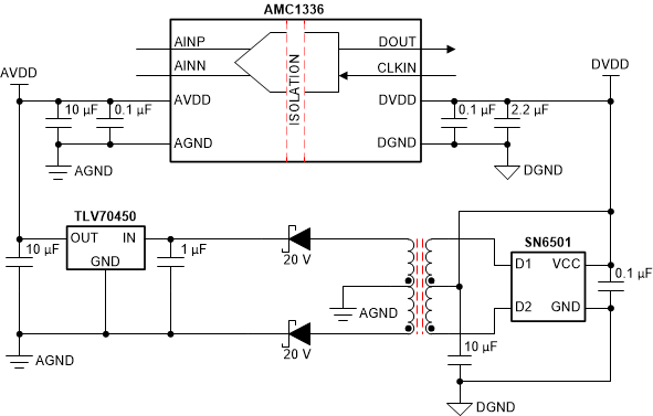
In a typical frequency-inverter application, the high-side power supply (AVDD) for the AMC1336 is generated from the controller-side supply (DVDD) of the device by an isolated dc/dc converter circuit. Figure 53 shows a low-cost solution based on the push-pull driver SN6501 and a transformer that supports the desired isolation voltage ratings. TI recommends using a low-ESR decoupling capacitor of 0.1 µF and an additional capacitor of minimum 1 µF for both supplies of the AMC1336. Place these decoupling capacitors as close as possible to the device power-supply pins to minimize supply current loops and electromagnetic emissions.
The AMC1336 does not require any specific power up sequencing. Consider the analog settling time tASTART as specified in the Table 10 table after ramp up of the AVDD high-side supply.
Connect the high-side ground pin AGND of the AMC1336 to one of the analog inputs AINx to avoid common-mode input voltage range violations.
 Figure 53. Decoupling the AMC1336