ZHCSK30B August 2019 – April 2020 AMC1336
PRODUCTION DATA.
- 1 特性
- 2 应用
- 3 说明
- 4 修订历史记录
- 5 Pin Configuration and Functions
-
6 Specifications
- Table 1. Absolute Maximum Ratings
- Table 2. ESD Ratings
- Table 3. Recommended Operating Conditions
- Table 4. Thermal Information
- Table 5. Power Ratings
- Table 6. Insulation Specifications
- Table 7. Safety-Related Certifications
- Table 8. Safety Limiting Values
- Table 9. Electrical Characteristics
- Table 10. Switching Characteristics
- 6.1 Insulation Characteristics Curves
- 6.2 Typical Characteristics
- 7 Detailed Description
- 8 Application and Implementation
- 9 Power Supply Recommendations
- 10Layout
- 11器件和文档支持
- 12机械、封装和可订购信息
7.3.1 Analog Input
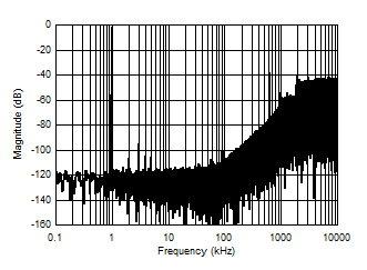
The AMC1336 incorporates front-end circuitry that contains an instrumentation amplifier, followed by a ΔΣ modulator. To support a bipolar input range with a unipolar high-side supply AVDD, the device uses a charge pump to simplify the overall system design and minimize circuit cost. For reduced offset and offset drift, the input buffer is chopper-stabilized with the switching frequency set at fCLKIN / 32. Figure 39 illustrates the spur created by the switching frequency.

| sinc3 filter, OSR = 1, fCLKIN = 20 MHz, fIN = 1 kHz |
The linearity and noise performance of the device are ensured only when the differential analog input voltage remains within the specified linear full-scale range (FSR), that is ±1 V, and within the specified input common-mode range.
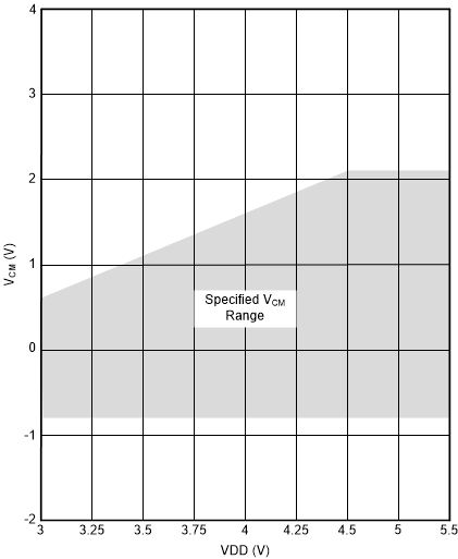
Figure 40 shows the specified common-mode input voltage that applies for the full-scale input voltage range as specified in this document.
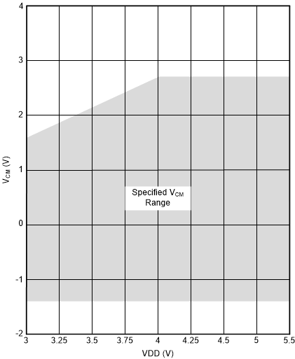
If smaller input signals are used, the operational common-mode input voltage range widens. Figure 41 shows the common-mode input voltage that applies with no differential input signal; that is, when the voltage applied on AINP is equal to the voltage applied on AINN. The common-mode input voltage range scales with the actual differential input voltage between this range and the range in Figure 40.

Clipping Differential Input Signal of ±1.25 V

Zero Differential Input Signal
There are two restrictions on the analog input signals (AINP and AINN). First, if the input voltage exceeds the range AGND – 5 V to AVDD + 0.5 V, the input current must be limited to 10 mA because the device input electrostatic discharge (ESD) diodes turn on. In addition, the linearity and noise performance of the device are ensured only when the differential analog input voltage remains within the specified linear full-scale range (FSR) and within the specified input common-mode range.