ZHCS161D April 2011 – July 2015 AMC1200
PRODUCTION DATA.
- 1 特性
- 2 应用
- 3 说明
- 4 修订历史记录
- 5 Pin Configuration and Functions
- 6 Specifications
- 7 Detailed Description
- 8 Application and Implementation
- 9 Power Supply Recommendations
- 10Layout
- 11器件和文档支持
- 12机械、封装和可订购信息
封装选项
机械数据 (封装 | 引脚)
散热焊盘机械数据 (封装 | 引脚)
- DUB|8
订购信息
7 Detailed Description
7.1 Overview
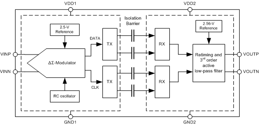
The AMC1200 is a fully-differential precision isolation amplifier. The analog input signal is converted to a digital signal and then transferred across a capacitive isolation barrier. The digital modulation used in the AMC1200 together with the isolation barrier characteristics result in excellent reliability and transient immunity.
After processing the digital signal with a low-pass filter, an analog signal is provided at the outputs. The main building blocks are shown in the Functional Block Diagram section.
The SiO2-based capacitive isolation barrier supports a high level of magnetic field immunity, as described in application report, ISO72x Digital Isolator Magnetic-Field Immunity (SLLA181), available for download at www.ti.com.
7.2 Functional Block Diagram

7.3 Feature Description
7.3.1 Insulation Characteristics
| PARAMETER | TEST CONDITIONS | MIN | TYP | MAX | UNIT | ||
|---|---|---|---|---|---|---|---|
| VIORM | Maximum working insulation voltage | 1200 | VPEAK | ||||
| VPR | Input to output test voltage | Qualification test: after Input/Output Safety Test Subgroup 2/3 VPR = VIORM × 1.2, t = 10 s, partial discharge < 5 pC | 1140 | VPEAK | |||
| Qualification test: method a, after environmental tests subgroup 1, VPR = VIORM × 1.6, t = 10 s, partial discharge < 5 pC | 1920 | VPEAK | |||||
| 100% production test: method b1, VPR = VIORM x 1.875, t = 1 s, partial discharge < 5 pC |
2250 | VPEAK | |||||
| VIOTM | Transient overvoltage | Qualification test: t = 60 s | AMC1200 | 4000 | VPEAK | ||
| AMC1200B | 4250 | VPEAK | |||||
| VISO | Insulation voltage per UL | Qualification test: VTEST = VISO, t = 60 s | AMC1200 | 4000 | VPEAK | ||
| AMC1200B | 4250 | VPEAK | |||||
| 100% production test: VTEST = 1.2 x VISO, t = 1 s | AMC1200 | 4800 | VPEAK | ||||
| AMC1200B | 5100 | VPEAK | |||||
| RS | Insulation resistance | VIO = 500 V at TS | > 109 | Ω | |||
| PD | Pollution degree | 2 | ° | ||||
7.3.2 IEC 61000-4-5 Ratings
7.3.3 IEC 60664-1 Ratings(1)
| PARAMETER | TEST CONDITIONS | SPECIFICATION |
|---|---|---|
| Basic isolation group | Material group | II |
| Installation classification | Rated mains voltage ≤ 150 VRMS | I-IV |
| Rated mains voltage ≤ 300 VRMS | I-IV | |
| Rated mains voltage ≤ 400 VRMS | I-III | |
| Rated mains voltage < 600 VRMS | I-III |
7.3.4 Package Characteristics(1)
7.3.5 IEC Safety Limiting Values
Safety limiting intends to prevent potential damage to the isolation barrier upon failure of input or output (I/O) circuitry. A failure of the I/O circuitry can allow low resistance to ground or the supply and, without current limiting, dissipate sufficient power to overheat the die and damage the isolation barrier, potentially leading to secondary system failures.
| PARAMETER | TEST CONDITIONS | MIN | TYP | MAX | UNIT | |
|---|---|---|---|---|---|---|
| IS | Safety input, output, or supply current | θJA = 246°C/W, VIN = 5.5 V, TJ = 150°C, TA = 25°C | 10 | mA | ||
| TC | Maximum case temperature | 150 | °C | |||
The safety-limiting constraint is the operating virtual junction temperature range specified in the Absolute Maximum Ratings table. The power dissipation and junction-to-air thermal impedance of the device installed in the application hardware determine the junction temperature. The assumed junction-to-air thermal resistance in the Thermal Information table is that of a device installed in the JESD51-3, Low Effective Thermal Conductivity Test Board for Leaded Surface Mount Packages and is conservative. The power is the recommended maximum input voltage times the current. The junction temperature is then the ambient temperature plus the power times the junction-to-air thermal resistance.
7.3.6 Regulatory Information
| VDE/IEC | UL |
|---|---|
| Certified according to VDE V 0884-10 | Recognized under 1577 component recognition program |
| Certificate number: 40016131 | File number: E181974 |
7.3.7 Isolation Amplifier
The AMC1200 device consists of a second order delta-sigma modulator input stage including an internal reference and clock generator. The output of the modulator and clock signal are differentially transmitted over the integrated capacitive isolation barrier that separates the high- and low-voltage domains. The received bitstream and clock signals are synchronized and processed by a third-order analog filter with a nominal gain of 8 on the low-side and presented as a differential output of the device, as shown in Functional Block Diagram section.
7.3.8 Analog Input
The analog input range is tailored to directly accommodate a voltage drop across a shunt resistor used for current sensing. However, there are two restrictions on the analog input signals, VINP and VINN. If the input voltage exceeds the range AGND – 0.5 V to AVDD + 0.5 V, the input current must be limited to 10 mA to prevent the implemented input protection diodes from damage. In addition, the linearity and the noise performance of the device are ensured only when the differential analog input voltage remains within ±250 mV.
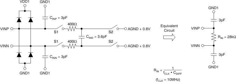
The differential analog input of the AMC1200 and AMC1200B devices is a switched-capacitor circuit based on a second-order modulator stage that digitizes the input signal into a 1-bit output stream. These devices compare the differential input signal (VIN = VINP – VINN) against the internal reference of 2.5 V using internal capacitors that are continuously charged and discharged with a typical frequency of 10 MHz. With the S1 switches closed, CIND charges to the voltage difference across VINP and VINN. For the discharge phase, both S1 switches open first and then both S2 switches close. CIND discharges to approximately AGND + 0.8 V during this phase. Figure 31 shows the simplified equivalent input circuitry.
 Figure 31. Equivalent Input Circuit
7.4 Device Functional Modes
The AMC1200 is operational when the power supplies VDD1 and VDD2 are applied as specified in the Recommended Operating Conditions section.
The AMC1200 does not have any additional functional modes.