ZHCSCL7C May   2014  – April 2021 AFE4403

PRODUCTION DATA  

  1. 特性
  2. 应用
  3. 说明
  4. Revision History
  5. Device Family Options
  6. Pin Configuration and Functions
  7. Specifications
    1. 7.1 Absolute Maximum Ratings
    2. 7.2 ESD Ratings
    3. 7.3 Recommended Operating Conditions
    4. 7.4 Thermal Information
    5. 7.5 Electrical Characteristics
    6. 7.6 Timing Requirements
    7. 7.7 Timing Requirements: Supply Ramp and Power-Down
    8. 7.8 Typical Characteristics
  8. Detailed Description
    1. 8.1 Overview
    2. 8.2 Functional Block Diagram
    3. 8.3 Feature Description
      1. 8.3.1 Receiver Channel
        1. 8.3.1.1 Receiver Front-End
        2. 8.3.1.2 Ambient Cancellation Scheme and Second Stage Gain Block
        3. 8.3.1.3 Receiver Control Signals
        4. 8.3.1.4 Receiver Timing
      2. 8.3.2 Clocking and Timing Signal Generation
      3. 8.3.3 Timer Module
        1. 8.3.3.1 Using the Timer Module
      4. 8.3.4 Receiver Subsystem Power Path
      5. 8.3.5 Transmit Section
        1. 8.3.5.1 Third LED Support
        2. 8.3.5.2 Transmitter Power Path
        3. 8.3.5.3 LED Power Reduction During Periods of Inactivity
        4. 8.3.5.4 LED Configurations
    4. 8.4 Device Functional Modes
      1. 8.4.1 ADC Operation and Averaging Module
        1. 8.4.1.1 Operation Without Averaging
        2. 8.4.1.2 Operation With Averaging
        3. 8.4.1.3 Dynamic Power-Down Mode
      2. 8.4.2 Diagnostics
        1. 8.4.2.1 Photodiode-Side Fault Detection
        2. 8.4.2.2 Transmitter-Side Fault Detection
        3. 8.4.2.3 Diagnostics Module
    5. 8.5 Programming
      1. 8.5.1 Serial Programming Interface
      2. 8.5.2 Reading and Writing Data
        1. 8.5.2.1 Writing Data
        2. 8.5.2.2 Reading Data
        3. 8.5.2.3 Multiple Data Reads and Writes
        4. 8.5.2.4 Register Initialization
        5. 8.5.2.5 AFE SPI Interface Design Considerations
    6. 8.6 Register Maps
      1. 8.6.1 AFE Register Map
      2. 8.6.2 AFE Register Description
  9. Application Information Disclaimer
    1. 9.1 Application Information
    2. 9.2 Typical Application
      1. 9.2.1 Design Requirements
      2. 9.2.2 Detailed Design Procedure
      3. 9.2.3 Application Curves
  10. 10Power Supply Recommendations
    1. 10.1 Power Consumption Considerations
  11. 11Layout
    1. 11.1 Layout Guidelines
    2. 11.2 Layout Example
  12. 12Device and Documentation Support
    1. 12.1 Trademarks
    2. 12.2 静电放电警告
    3. 12.3 术语表
  13. 13Mechanical, Packaging, and Orderable Information

封装选项

机械数据 (封装 | 引脚)
散热焊盘机械数据 (封装 | 引脚)
订购信息

Operation With Averaging

In this mode, all ADC digital samples are accumulated and averaged after every 50 µs. At each rising edge of the ADC reset signal, one averaged ADC conversion value is written into the output registers sequentially, as follows (see Figure 8-29):

  • At the 25% reset signal, the first averaged ADC sample is written to register 2Ah (Decimal address = 42).
  • At the 50% reset signal, the second averaged ADC sample is written to register 2Bh (Decimal address = 43).
  • At the 75% reset signal, the third averaged ADC sample is written to register 2Ch (Decimal address = 44).
  • At the next 0% reset signal, the fourth averaged ADC sample is written to register 2Dh (Decimal address = 45).
  • Every time the registers 2Ah and 2Bh are updated, the contents of the difference register 2Eh is updated. Similarly, every time the registers 2Ch and 2Dh are updated, the contents of the difference register 2Fh is updated.

The number of samples to be used per conversion phase is specified in the CONTROL1 register (NUMAV[7:0]). The user must specify the correct value for the number of averages, as described in Equation 6:

Equation 6. GUID-BCE22DDB-9BE7-4BAD-8387-761B82E00F10-low.gif

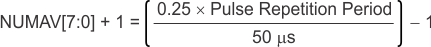
Note that the 50-µs factor corresponds to a case where the internal clock of the AFE (after division) is exactly equal to 4 MHz. The factor scales linearly with the clock period being used.

Note that the number of average conversions is limited by 25% of the PRF. For example, eight samples can be averaged with PRF = 625 Hz, and four samples can be averaged with PRF = 1250 Hz.

GUID-20201119-CA0I-2RFP-BJHH-C4HWVZKFRCHK-low.gif Figure 8-28 ADC Data Without Averaging (When Number of Averages = 0)
Note: Every time Register 2Ah or Register 2Bh are updated, the difference (Register 2Ah - register 2Bh) is written into register 2Eh. Every time Register 2Ch or Register 2Dh are updated, the difference (Register 2Ch - register 2Dh) is written into register 2Fh.
GUID-20210106-CA0I-PQRH-QRNX-PXTVFJHD883F-low.gif
NOTE: Example is with three averages. The value of the NUMAVG[7:0] register bits = 2.
Figure 8-29 ADC Data with Averaging Enabled
Note: Every time Register 2Ah or Register 2Bh are updated, the difference (Register 2Ah - register 2Bh) is written into register 2Eh. Every time Register 2Ch or Register 2Dh are updated, the difference (Register 2Ch - register 2Dh) is written into register 2Fh.