SBAS363E December 2009 – August 2016 ADS8331 , ADS8332
PRODUCTION DATA.
- 1 Features
- 2 Applications
- 3 Description
- 4 Revision History
- 5 Companion Products
- 6 Device Comparison
- 7 Pin Configuration and Functions
-
8 Specifications
- 8.1 Absolute Maximum Ratings
- 8.2 ESD Ratings
- 8.3 Recommended Operating Conditions
- 8.4 Thermal Information
- 8.5 Electrical Characteristics: VA = 2.7 V
- 8.6 Electrical Characteristics: VA = 5 V
- 8.7 Timing Requirements: VA = 2.7 V
- 8.8 Timing Characteristics: VA = 5 V
- 8.9 Typical Characteristics: DC Performance
- 8.10 Typical Characteristics: AC Performance
- 9 Detailed Description
- 10Application and Implementation
- 11Power Supply Recommendations
- 12Layout
- 13Device and Documentation Support
- 14Mechanical, Packaging, and Orderable Information
封装选项
机械数据 (封装 | 引脚)
散热焊盘机械数据 (封装 | 引脚)
- RGE|24
订购信息
8 Specifications
8.1 Absolute Maximum Ratings
over operating free-air temperature range (unless otherwise noted)(1)(1) Stresses beyond those listed under Absolute Maximum Ratings may cause permanent damage to the device. These are stress ratings only, and functional operation of the device at these or any other conditions beyond those indicated is not implied. Exposure to absolute-maximum-rated conditions for extended periods may affect device reliability.
8.2 ESD Ratings
| VALUE | UNIT | |||
|---|---|---|---|---|
| V(ESD) | Electrostatic discharge | Human-body model (HBM), per ANSI/ESDA/JEDEC JS-001(1) | ±2000 | V |
| Charged-device model (CDM), per JEDEC specification JESD22-C101(2) | ±500 | |||
(1) JEDEC document JEP155 states that 500-V HBM allows safe manufacturing with a standard ESD control process.
(2) JEDEC document JEP157 states that 250-V CDM allows safe manufacturing with a standard ESD control process.
8.3 Recommended Operating Conditions
over operating free-air temperature range (unless otherwise noted)| MIN | NOM | MAX | UNIT | ||
|---|---|---|---|---|---|
| VA | Analog supply voltage | 2.7 | 3 | 5.5 | V |
| VBD | Digital supply voltage | 1.65 | 3 | VA + 0.2 | V |
8.4 Thermal Information
| THERMAL METRIC(1) | ADS833x | UNIT | ||
|---|---|---|---|---|
| RGE (VQFN) | PW (TSSOP) | |||
| 24 PINS | 24 PINS | |||
| RθJA | Junction-to-ambient thermal resistance | 31.9 | 78.3 | °C/W |
| RθJC(top) | Junction-to-case (top) thermal resistance | 29.2 | 12.1 | °C/W |
| RθJB | Junction-to-board thermal resistance | 8.7 | 33.8 | °C/W |
| ψJT | Junction-to-top characterization parameter | 0.3 | 0.3 | °C/W |
| ψJB | Junction-to-board characterization parameter | 8.7 | 33.5 | °C/W |
| RθJC(bot) | Junction-to-case (bottom) thermal resistance | 2.25 | NA | °C/W |
(1) For more information about traditional and new thermal metrics, see the Semiconductor and IC Package Thermal Metrics application report, SPRA953.
8.5 Electrical Characteristics: VA = 2.7 V
at TA = –40°C to 85°C, VA = 2.7 V, VBD = 1.65 V to 2.7 V, VREF = 2.5 V, and fSAMPLE = 500 kSPS (unless otherwise noted)| PARAMETER | TEST CONDITIONS | MIN | TYP | MAX | UNIT | |||
|---|---|---|---|---|---|---|---|---|
| ANALOG INPUT | ||||||||
| Full-scale input voltage (1) | INX – COM, ADCIN – COM | 0 | VREF | V | ||||
| Absolute input voltage | INX, ADCIN | AGND – 0.2 | VA + 0.2 | V | ||||
| COM | AGND – 0.2 | AGND + 0.2 | ||||||
| Input capacitance | ADCIN | 40 | 45 | pF | ||||
| Input leakage current | Unselected ADC input | ±1 | nA | |||||
| SYSTEM PERFORMANCE | ||||||||
| Resolution | 16 | Bits | ||||||
| No missing codes | 16 | Bits | ||||||
| INL | Integral linearity | ADS8331I, ADS8332I | –3 | ±2 | 3 | LSB(2) | ||
| ADS8331IB, ADS8332IB | –2 | ±1.2 | 2 | |||||
| DNL | Differential linearity | ADS8331I, ADS8332I | –1 | ±0.6 | 2 | LSB(2) | ||
| ADS8331IB, ADS8332IB | –1 | ±0.6 | 1.5 | |||||
| EO | Offset error(3) | –0.5 | ±0.15 | 0.5 | mV | |||
| Offset error drift | ±1 | PPM/°C | ||||||
| Offset error matching | –0.2 | 0.2 | mV | |||||
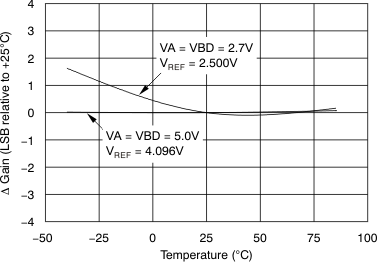
| EG | Gain error | –0.25 | –0.06 | 0.25 | %FSR | |||
| Gain error drift | ±0.4 | PPM/°C | ||||||
| Gain error matching | –0.003 | 0.003 | %FSR | |||||
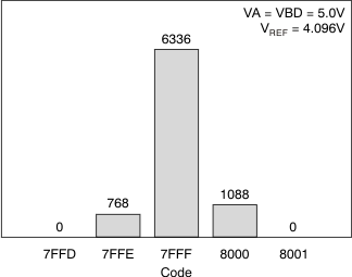
| Transition noise | 28 | μV RMS | ||||||
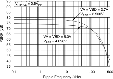
| PSRR | Power-supply rejection ratio | 74 | dB | |||||
| SAMPLING DYNAMICS | ||||||||
| tCONV | Conversion time | 18 | CCLK | |||||
| tSAMPLE1 | Acquisition time | Manual-trigger mode | 3 | CCLK | ||||
| tSAMPLE2 | Auto-trigger mode | 3 | ||||||
| Throughput rate | 500 | kSPS | ||||||
| DYNAMIC CHARACTERISTICS | ||||||||
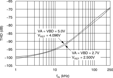
| THD | Total harmonic distortion (4) | VIN = 2.5 VPP at 1 kHz | –101 | dB | ||||
| VIN = 2.5 VPP at 10 kHz | –95 | |||||||
| SNR | Signal-to-noise ratio | VIN = 2.5 VPP at 1 kHz | ADS8331I, ADS8332I | 88 | dB | |||
| ADS8331IB, ADS8332IB | 89 | |||||||
| VIN = 2.5 VPP at 10 kHz | ADS8331I, ADS8332I | 86.5 | ||||||
| ADS8331IB, ADS8332IB | 87.5 | |||||||
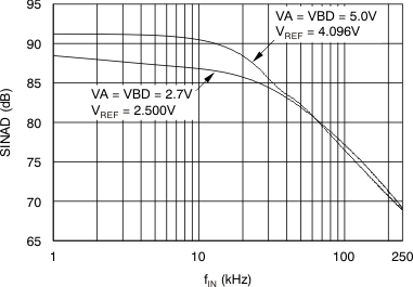
| SINAD | Signal-to-noise + distortion | VIN = 2.5 VPP at 1 kHz | ADS8331I, ADS8332I | 87.5 | dB | |||
| ADS8331IB, ADS8332IB | 88.5 | |||||||
| VIN = 2.5 VPP at 10 kHz | ADS8331I, ADS8332I | 86 | ||||||
| ADS8331IB, ADS8332IB | 87 | |||||||
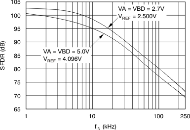
| SFDR | Spurious-free dynamic range | VIN = 2.5 VPP at 1 kHz | 103 | dB | ||||
| VIN = 2.5 VPP at 10 kHz | 98 | |||||||
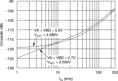
| Crosstalk | VIN = 2.5 VPP at 1 kHz | 125 | dB | |||||
| VIN = 2.5 VPP at 100 kHz | 108 | |||||||
| –3-dB small-signal bandwidth | INX – COM with MUXOUT tied to ADCIN | 17 | MHz | |||||
| ADCIN – COM | 30 | |||||||
| CLOCK | ||||||||
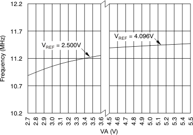
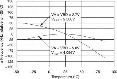
| Internal conversion clock frequency | 10.5 | 11 | 12.2 | MHz | ||||
| SCLK external serial clock | Used as I/O clock only | 25 | MHz | |||||
| Used as both I/O clock and conversion clock | 1 | 21 | MHz | |||||
| EXTERNAL VOLTAGE REFERENCE INPUT | ||||||||
| VREF | Input reference range(5) | (REF+) – (REF–) | 1.2 | 2.525 | V | |||
| (REF–) – AGND | –0.1 | 0.1 | ||||||
| Resistance (6) | Reference input | 20 | kΩ | |||||
| DIGITAL INPUT/OUTPUT | ||||||||
| Logic family | CMOS | |||||||
| VIH | High-level input voltage | 1.65 V < VBD < 2.5 V | 0.8 × VBD | VBD + 0.3 | V | |||
| 2.5 V ≤ VBD ≤ VA | 0.65 × VBD | VBD + 0.3 | ||||||
| VIL | Low-level input voltage | 1.65 < VBD < 2.5 V | –0.3 | 0.1 × VBD | V | |||
| 2.5 V ≤ VBD ≤ VA | –0.3 | 0.25 × VBD | ||||||
| II | Input current | VIN = VBD or DGND | –1 | 1 | μA | |||
| CI | Input capacitance | 5 | pF | |||||
| VOH | High-level output voltage | VA ≥ VBD ≥ 1.65V, IO = 100 μA | VBD – 0.6 | VBD | V | |||
| VOL | Low-level output voltage | VA ≥ VBD ≥ 1.65 V, IO = –100 μA | 0 | 0.4 | V | |||
| CO | SDO pin capacitance | Hi-Z state | 5 | pF | ||||
| CL | Load capacitance | 30 | pF | |||||
| Data format | Straight binary | |||||||
| POWER-SUPPLY REQUIREMENTS | ||||||||
| VA | Analog supply voltage(5) | 2.7 | 3.6 | V | ||||
| VBD | Digital I/O supply voltage | 1.65 | VA + 0.2 | V | ||||
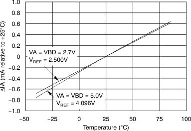
| IA | Analog supply current | fSAMPLE = 500 kSPS | 5.2 | 6.5 | mA | |||
| fSAMPLE = 250 kSPS in Auto-NAP mode | 3.2 | |||||||
| Nap mode, SCLK = VBD or DGND | 325 | 400 | μA | |||||
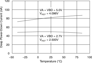
| Deep PD mode, SCLK = VBD or DGND | 50 | 250 | nA | |||||
| IBD | Digital I/O supply current | fSAMPLE = 500 kilobytes per second | 0.1 | 0.4 | mA | |||
| fSAMPLE = 250 kSPS in Auto-NAP mode | 0.05 | |||||||
| Power dissipation | VA = 2.7 V, VBD = 1.65 V, fSAMPLE = 500 kSPS | 14.2 | 18.2 | mW | ||||
| VA = 2.7V, VBD = 1.65 V, fSAMPLE = 250 kSPS in Auto-NAP mode | 8.72 | |||||||
| TEMPERATURE RANGE | ||||||||
| TA | Operating free-air temperature | –40 | 85 | °C | ||||
(1) Ideal input span; does not include gain or offset error.
(2) LSB means least significant bit.
(3) Measured relative to an ideal full-scale input (INX – COM) of 2.5 V when VA = 2.7 V.
(4) Calculated on the first nine harmonics of the input frequency.
(5) The ADS8331, ADS8332 operates with VA from 2.7 V to 5.5 V, and VREF between 1.2 V and VA. However, the device may not meet the specifications listed in the Electrical Characteristics when VA is from 3.6 V to 4.5 V.
(6) Can vary ±30%.
8.6 Electrical Characteristics: VA = 5 V
at TA = –40°C to 85°C, VA = 5 V, VBD = 1.65 V to 5 V, VREF = 4.096 V, and fSAMPLE = 500 kSPS (unless otherwise noted)| PARAMETER | TEST CONDITIONS | MIN | TYP | MAX | UNIT | |||
|---|---|---|---|---|---|---|---|---|
| ANALOG INPUT | ||||||||
| Full-scale input voltage (1) | INX – COM, ADCIN – COM | 0 | VREF | V | ||||
| Absolute input voltage | INX, ADCIN | AGND – 0.2 | VA + 0.2 | V | ||||
| COM | AGND – 0.2 | AGND + 0.2 | ||||||
| Input capacitance | ADCIN | 40 | 45 | pF | ||||
| Input leakage current | Unselected ADC input | ±1 | nA | |||||
| SYSTEM PERFORMANCE | ||||||||
| Resolution | 16 | Bits | ||||||
| No missing codes | 16 | Bits | ||||||
| INL | Integral linearity | ADS8331I, ADS8332I | –3 | ±2 | 3 | LSB(2) | ||
| ADS8331IB, ADS8332IB | –2 | ±1 | 2 | |||||
| DNL | Differential linearity | ADS8331I, ADS8332I | –1 | ±1 | 2 | LSB(2) | ||
| ADS8331IB, ADS8332IB | –1 | ±0.5 | 1.5 | |||||
| EO | Offset error(3) | –1 | ±0.23 | 1 | mV | |||
| Offset error drift | ±1 | PPM/°C | ||||||
| Offset error matching | –0.125 | 0.125 | mV | |||||
| EG | Gain error | –0.25 | –0.06 | 0.25 | %FSR | |||
| Gain error drift | ±0.02 | PPM/°C | ||||||
| Gain error matching | –0.003 | 0.003 | %FSR | |||||
| Transition noise | 30 | μV RMS | ||||||
| PSRR | Power-supply rejection ratio | 78 | dB | |||||
| SAMPLING DYNAMICS | ||||||||
| tCONV | Conversion time | 18 | CCLK | |||||
| tSAMPLE1 | Acquisition time | Manual-trigger mode | 3 | CCLK | ||||
| tSAMPLE2 | Auto-trigger mode | 3 | ||||||
| Throughput rate | 500 | kSPS | ||||||
| DYNAMIC CHARACTERISTICS | ||||||||
| THD | Total harmonic distortion (4) | VIN = 4.096 VPP at 1 kHz | –100 | dB | ||||
| VIN = 4.096 VPP at 10 kHz | ADS8331I, ADS8332I | –94 | ||||||
| ADS8331IB, ADS8332IB | –95 | |||||||
| SNR | Signal-to-noise ratio | VIN = 4.096 VPP at 1 kHz | ADS8331I, ADS8332I | 90.5 | dB | |||
| ADS8331IB, ADS8332IB | 91.5 | |||||||
| VIN = 4.096 VPP at 10 kHz | 88 | |||||||
| SINAD | Signal-to-noise + distortion | VIN = 4.096 VPP at 1 kHz | ADS8331I, ADS8332I | 90 | dB | |||
| ADS8331IB, ADS8332IB | 91 | |||||||
| VIN = 4.096 VPP at 10 kHz | 87 | |||||||
| SFDR | Spurious-free dynamic range | VIN = 4.096 VPP at 1 kHz | 101 | dB | ||||
| VIN = 4.096 VPP at 10 kHz | 96 | |||||||
| Crosstalk | VIN = 4.096 VPP at 1 kHz | 119 | dB | |||||
| VIN = 4.096 VPP at 100 kHz | 107 | |||||||
| –3-dB small-signal bandwidth | INX – COM with MUXOUT tied to ADCIN | 22 | MHz | |||||
| ADCIN – COM | 40 | |||||||
| CLOCK | ||||||||
| Internal conversion clock frequency | 10.9 | 11.5 | 12.6 | MHz | ||||
| SCLK external serial clock | Used as I/O clock only | 40 | MHz | |||||
| Used as both I/O clock and conversion clock | 1 | 21 | ||||||
| EXTERNAL VOLTAGE REFERENCE INPUT | ||||||||
| VREF | Input reference range(5) | (REF+) – (REF–) | 1.2 | 4.096 | 4.2 | V | ||
| (REF–) – AGND | –0.1 | 0.1 | ||||||
| Resistance (6) | Reference input | 20 | kΩ | |||||
| DIGITAL INPUT/OUTPUT | ||||||||
| Logic family | CMOS | |||||||
| VIH | High-level input voltage | 1.65 < VBD < 2.5 V | 0.8 × VBD | VBD + 0.3 | V | |||
| 2.5 V ≤ VBD ≤ VA | 0.65 × VBD | VBD + 0.3 | ||||||
| VIL | Low-level input voltage | 1.65 < VBD < 2.5 V | –0.3 | 0.1 × VBD | V | |||
| 2.5 V ≤ VBD ≤ VA | –0.3 | 0.25 × VBD | ||||||
| II | Input current | VIN = VBD or DGND | –1 | 1 | µA | |||
| CI | Input capacitance | 5 | pF | |||||
| VOH | High-level output voltage | VA ≥ VBD ≥ 1.65 V, IO = 100 μA | VBD – 0.6 | VBD | V | |||
| VOL | Low-level output voltage | VA ≥ VBD ≥ 1.65 V, IO = –100 μA | 0 | 0.4 | V | |||
| CO | SDO pin capacitance | Hi-Z state | 5 | pF | ||||
| CL | Load capacitance | 30 | pF | |||||
| Data format | Straight binary | |||||||
| POWER-SUPPLY REQUIREMENTS | ||||||||
| VA | Analog supply voltage(5) | 4.5 | 5 | 5.5 | V | |||
| VBD | Digital I/O supply voltage | 1.65 | VA + 0.2 | V | ||||
| IA | Analog supply current | fSAMPLE = 500 kSPS | 6.6 | 7.75 | mA | |||
| fSAMPLE = 250 kSPS in Auto-NAP mode | 4.2 | |||||||
| Nap mode, SCLK = VBD or DGND | 390 | 500 | μA | |||||
| Deep PD mode, SCLK = VBD or DGND | 80 | 250 | nA | |||||
| IBD | Digital I/O supply current | fSAMPLE = 500 kSPS | 1.2 | 2 | mA | |||
| fSAMPLE = 250 kSPS in Auto-NAP mode | 0.7 | |||||||
| Power dissipation | VA = 5 V, VBD = 5 V, fSAMPLE = 500 kSPS | 39 | 48.75 | mW | ||||
| VA = 5 V, VBD = 5 V, fSAMPLE = 250 kSPS in Auto-NAP mode | 24.5 | |||||||
| TEMPERATURE RANGE | ||||||||
| TA | Operating free-air temperature | –40 | 85 | °C | ||||
(1) Ideal input span; does not include gain or offset error.
(2) LSB means least significant bit.
(3) Measured relative to an ideal full-scale input (INX – COM) of 4.096 V when VA = 5 V.
(4) Calculated on the first nine harmonics of the input frequency.
(5) The ADS8331, ADS8332 operates with VA from 2.7 V to 5.5 V, and VREF between 1.2 V and VA. However, the device may not meet the specifications listed in the Electrical Characteristics when VA is from 3.6 V to 4.5 V.
(6) Can vary ±30%.
8.7 Timing Requirements: VA = 2.7 V
at TA = –40°C to 85°C, VA = 2.7 V, and VBD = 1.65 V (unless otherwise noted)(1)(2)| MIN | NOM | MAX | UNIT | |||
|---|---|---|---|---|---|---|
| fCCLK | Frequency, conversion clock, CCLK | External, fCCLK = 1/2 fSCLK | 0.5 | 10.5 | MHz | |
| Internal | 10.5 | 11 | 12.2 | |||
| tSU1 | Setup time, rising edge of CS to EOC(4) | Read while converting | 1 | CCLK | ||
| tH1 | CS hold time with respect to EOC(4) | Read while sampling | 25 | ns | ||
| tWL1 | Pulse duration, CONVST low | 40 | ns | |||
| tWH1 | Pulse duration, CS high | 40 | ns | |||
| tSU2 | Setup time, rising edge of CS to EOS | Read while sampling | 25 | ns | ||
| tH2 | CS hold time with respect to EOS | Read while converting | 25 | ns | ||
| tSU3 | Setup time, falling edge of CS to first falling edge of SCLK | 14 | ns | |||
| tWL2 | Pulse duration, SCLK low | 17 | tSCLK – tWH2 | ns | ||
| tWH2 | Pulse duration, SCLK high | 12 | tSCLK – tWL2 | ns | ||
| tSCLK | Cycle time, SCLK | I/O clock only | 40 | ns | ||
| I/O and conversion clocks | 47.6 | 1000 | ||||
| I/O clock, daisy-chain mode | 40 | |||||
| I/O and conversion clocks, daisy-chain mode | 47.6 | 1000 | ||||
| tD1 | Delay time, falling edge of SCLK to SDO invalid | 10-pF load | 8 | ns | ||
| tD2 | Delay time, falling edge of SCLK to SDO valid | 10-pF load | 35 | ns | ||
| tD3 | Delay time, falling edge of CS to SDO valid, SDO MSB output | 10-pF load | 35 | ns | ||
| tSU4 | Setup time, SDI to falling edge of SCLK | 8 | ns | |||
| tH3 | Hold time, SDI to falling edge of SCLK | 8 | ns | |||
| tD4 | Delay time, rising edge of CS to SDO 3-state | 10-pF load | 15 | ns | ||
| tSU5 | Setup time, last falling edge of SCLK before rising edge of CS | 15 | ns | |||
| tH4 | Hold time, last falling edge of SCLK before rising edge of CS | 2 | ns | |||
| tSU6(3) | Setup time, rising edge of SCLK to rising edge of CS | 10 | ns | |||
| tH5(3) | Hold time, rising edge of SCLK to rising edge of CS | 2 | ns | |||
| tD5 | Delay time, falling edge of CS to deactivation of INT | 10-pF load | 40 | ns | ||
(1) All input signals are specified with tr = tf = 1.5 ns (10% to 90% of VBD) and timed from a voltage level of (VIL + VIH) / 2.
(2) See the timing diagrams.
(3) Applies to the 5th or 17th rising SCLK when sending 4-bit or 16-bit commands, respectively, to the ADS8331, ADS8332.
(4) The EOC and EOS signals are the inverse of each other.
8.8 Timing Characteristics: VA = 5 V
at TA = –40°C to 85°C, and VA = VBD = 5 V (unless otherwise noted)(1)(2)| MIN | TYP | MAX | UNIT | |||
|---|---|---|---|---|---|---|
| fCCLK | Frequency, conversion clock, CCLK | External, fCCLK = 1/2 fSCLK | 0.5 | 10.5 | MHz | |
| Internal | 10.9 | 11.5 | 12.6 | |||
| tSU1 | Setup time, rising edge of CS to EOC(4) | Read while converting | 1 | CCLK | ||
| tH1 | CS hold time with respect to EOC(4) | Read while sampling | 20 | ns | ||
| tWL1 | Pulse duration, CONVST low | 40 | ns | |||
| tWH1 | Pulse duration, CS high | 40 | ns | |||
| tSU2 | Setup time, rising edge of CS to EOS | Read while sampling | 20 | ns | ||
| tH2 | CS hold time with respect to EOS | Read while converting | 20 | ns | ||
| tSU3 | Setup time, falling edge of CS to first falling edge of SCLK | 8 | ns | |||
| tWL2 | Pulse duration, SCLK low | 12 | tSCLK – tWH2 | ns | ||
| tWH2 | Pulse duration, SCLK high | 11 | tSCLK – tWL2 | ns | ||
| tSCLK | Cycle time, SCLK | I/O clock only | 25 | ns | ||
| I/O and conversion clocks | 47.6 | 1000 | ||||
| I/O clock, daisy-chain mode | 25 | |||||
| I/O and conversion clocks, daisy-chain mode | 47.6 | 1000 | ||||
| tD1 | Delay time, falling edge of SCLK to SDO invalid | 10-pF load | 5 | ns | ||
| tD2 | Delay time, falling edge of SCLK to SDO valid | 10-pF load | 20 | ns | ||
| tD3 | Delay time, falling edge of CS to SDO valid, SDO MSB output | 10-pF load | 20 | ns | ||
| tSU4 | Setup time, SDI to falling edge of SCLK | 8 | ns | |||
| tH3 | Hold time, SDI to falling edge of SCLK | 8 | ns | |||
| tD4 | Delay time, rising edge of CS to SDO 3-state | 10-pF load | 10 | ns | ||
| tSU5 | Setup time, last falling edge of SCLK before rising edge of CS | 10 | ns | |||
| tH4 | Hold time, last falling edge of SCLK before rising edge of CS | 2 | ns | |||
| tSU6(3) | Setup time, rising edge of SCLK to rising edge of CS | 10 | ns | |||
| tH5(3) | Hold time, rising edge of SCLK to rising edge of CS | 2 | ns | |||
| tD5 | Delay time, falling edge of CS to deactivation of INT | 10-pF load | 20 | ns | ||
(1) All input signals are specified with tr = tf = 1.5 ns (10% to 90% of VBD) and timed from a voltage level of (VIL + VIH) / 2.
(2) See the timing diagrams.
(3) Applies to the 5th or 17th rising SCLK when sending 4-bit or 16-bit commands, respectively, to the ADS8331, ADS8332.
(4) The EOC and EOS signals are the inverse of each other.
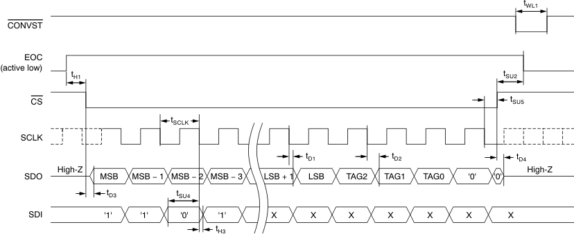
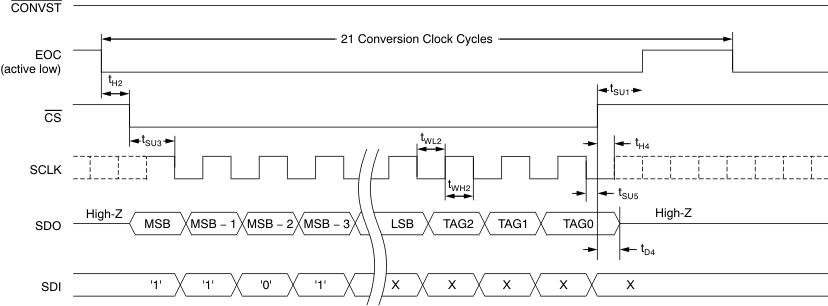 Figure 2. Read While Converting (Shown With Auto-Trigger Mode at 500 kSPS)
 Figure 4. Relationship among CS, EOC, and INT
8.9 Typical Characteristics: DC Performance
at TA = 25°C, VREF (REF+ – REF–) = 4.096 V when VA = VBD = 5 V or VREF (REF+ – REF–) = 2.5 V when VA = VBD = 2.7 V, fSCLK = 21 MHz, and fSAMPLE = 500 kSPS (unless otherwise noted)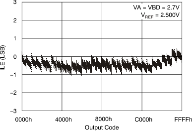
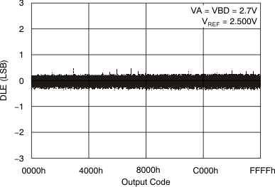
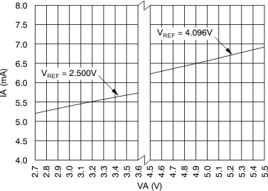
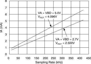
Analog Supply Voltage
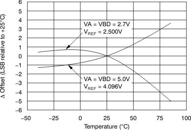
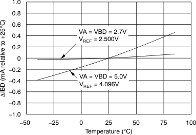
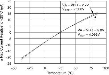
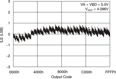
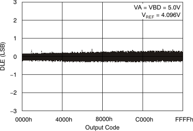
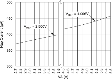
Analog Supply Voltage
8.10 Typical Characteristics: AC Performance
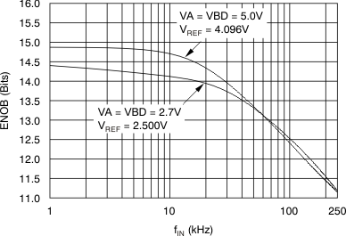
at TA = 25°C, VREF (REF+ – REF–) = 4.096 V when VA = VBD = 5 V or VREF (REF+ – REF–) = 2.5 V when VA = VBD = 2.7 V, fSCLK = 21 MHz, and fSAMPLE = 500 kSPS (unless otherwise noted)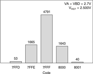
(8192 Conversions)
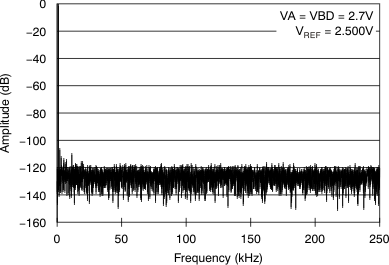
(8192 Point FFT, fIN = 1.0376 kHz, –0.2 dB)
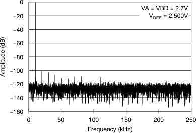
(8192 Point FFT, fIN = 10.0708 kHz, –0.2 dB)
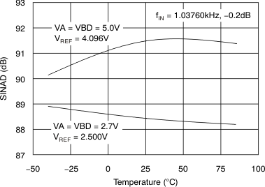
(8192 Conversions)
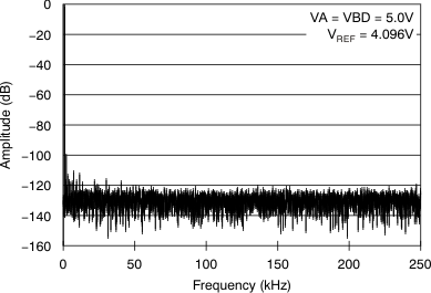
(8192 Point FFT, fIN = 1.0376 kHz, –0.2 dB)
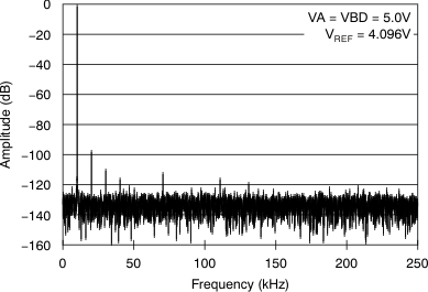
(8192 Point FFT, fIN = 10.0708 kHz, –0.2 dB)
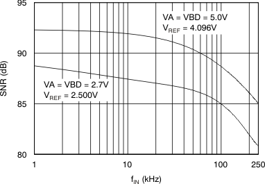
Input Frequency
