SBAS363E December 2009 – August 2016 ADS8331 , ADS8332
PRODUCTION DATA.
- 1 Features
- 2 Applications
- 3 Description
- 4 Revision History
- 5 Companion Products
- 6 Device Comparison
- 7 Pin Configuration and Functions
-
8 Specifications
- 8.1 Absolute Maximum Ratings
- 8.2 ESD Ratings
- 8.3 Recommended Operating Conditions
- 8.4 Thermal Information
- 8.5 Electrical Characteristics: VA = 2.7 V
- 8.6 Electrical Characteristics: VA = 5 V
- 8.7 Timing Requirements: VA = 2.7 V
- 8.8 Timing Characteristics: VA = 5 V
- 8.9 Typical Characteristics: DC Performance
- 8.10 Typical Characteristics: AC Performance
- 9 Detailed Description
- 10Application and Implementation
- 11Power Supply Recommendations
- 12Layout
- 13Device and Documentation Support
- 14Mechanical, Packaging, and Orderable Information
封装选项
机械数据 (封装 | 引脚)
散热焊盘机械数据 (封装 | 引脚)
- RGE|24
订购信息
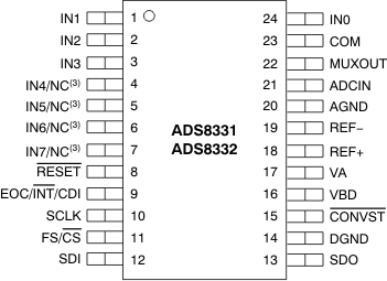
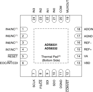
7 Pin Configuration and Functions
PW Package
24-Pin TSSOP
Top View

RGE Package
24-Pin VQFN With Exposed Thermal Pad
Top View

1. NC = No internal connection (ADS8331 only).
2. Connect thermal pad to analog ground.
3. NC = No internal connection (ADS8331 only).
Pin Functions: ADS8331
| PIN | I/O | DESCRIPTION | ||
|---|---|---|---|---|
| NAME | TSSOP | VQFN | ||
| ADCIN | 21 | 18 | I | ADC input |
| AGND | 20 | 17 | — | Analog ground |
| DGND | 14 | 11 | — | Digital interface ground |
| COM | 23 | 20 | I | Common ADC input (usually connected to AGND) |
| CONVST | 15 | 12 | I | Conversion start. Freezes sample and hold, starts conversion. |
| EOC/INT/CDI | 9 | 6 | O/O/I | Status output. If programmed as end-of-conversion (EOC), this pin is low (default) when a conversion is in progress. If programmed as an interrupt (INT), this pin is low (default) after the end of conversion and returns high after FS/CS goes low. The polarity of EOC or INT is programmable. This pin can also be used as a chain data input (CDI) when operated in daisy-chain mode. |
| FS/CS | 11 | 8 | I | Frame sync signal for DSP (such as TMS320™ DSP) or chip select input for SPI. |
| IN[0:3] | 1-3, 24 | 21-24 | I | Mux inputs |
| NC | 4-7 | 1-4 | — | No connection |
| MUXOUT | 22 | 19 | O | Mux output |
| REF+ | 18 | 15 | I | External reference input |
| REF– | 19 | 16 | — | External reference ground (connect to AGND through an individual via on the printed-circuit-board) |
| RESET | 8 | 5 | I | External reset (active low) |
| SCLK | 10 | 7 | I | SPI clock for serial interface |
| SDI | 12 | 9 | I | SPI serial data in |
| SDO | 13 | 10 | O | SPI serial data out |
| VA | 17 | 14 | — | Analog supply, 2.7 V to 5.5 V |
| VBD | 16 | 13 | — | Digital interface supply |
Pin Functions: ADS8332
| PIN | I/O | DESCRIPTION | ||
|---|---|---|---|---|
| NAME | TSSOP | VQFN | ||
| ADCIN | 21 | 18 | I | ADC input |
| AGND | 20 | 17 | — | Analog ground |
| DGND | 14 | 11 | — | Digital interface ground |
| COM | 23 | 20 | I | Common ADC input (usually connected to AGND) |
| CONVST | 15 | 12 | I | Conversion start. Freezes sample and hold, starts conversion. |
| EOC/INT/CDI | 9 | 6 | O/O/I | Status output. If programmed as end-of-conversion (EOC), this pin is low (default) when a conversion is in progress. If programmed as an interrupt (INT), this pin is low (default) after the end of conversion and returns high after FS/CS goes low. The polarity of EOC or INT is programmable. This pin can also be used as a chain data input (CDI) when operated in daisy-chain mode. |
| FS/CS | 11 | 8 | I | Frame sync signal for DSP (such as TMS320™ DSP) or chip select input for SPI. |
| IN[0:7] | 1-7, 24 | 1-4, 21-24 | I | Mux inputs |
| MUXOUT | 22 | 19 | O | Mux output |
| REF+ | 18 | 15 | I | External reference input |
| REF– | 19 | 16 | — | External reference ground (connect to AGND through an individual via on the printed-circuit-board) |
| RESET | 8 | 5 | I | External reset (active low) |
| SCLK | 10 | 7 | I | SPI clock for serial interface |
| SDI | 12 | 9 | I | SPI serial data in |
| SDO | 13 | 10 | O | SPI serial data out |
| VA | 17 | 14 | — | Analog supply, 2.7 V to 5.5 V |
| VBD | 16 | 13 | — | Digital interface supply |