SBAS108E May 2000 – December 2016 ADS8320
PRODUCTION DATA.
- 1 Features
- 2 Applications
- 3 Description
- 4 Revision History
- 5 Pin Configuration and Functions
- 6 Specifications
- 7 Detailed Description
- 8 Application and Implementation
- 9 Power Supply Recommendations
- 10Layout
- 11Device and Documentation Support
- 12Mechanical, Packaging, and Orderable Information
6 Specifications
6.1 Absolute Maximum Ratings
over operating free-air temperature range (unless otherwise noted)(1)| MIN | MAX | UNIT | ||
|---|---|---|---|---|
| VCC | 6 | V | ||
| Analog input | –0.3 | VCC + 0.3 | V | |
| Logic input | –0.3 | 6 | °C | |
| External reference voltage | 5.5 | V | ||
| Input current to any pin except supply | ±10 | mA | ||
| Case temperature | 100 | °C | ||
| Junction temperature | 150 | °C | ||
| Storage temperature, Tstg | 125 | °C | ||
(1) Stresses beyond those listed under Absolute Maximum Ratings may cause permanent damage to the device. These are stress ratings only, which do not imply functional operation of the device at these or any other conditions beyond those indicated under Recommended Operating Conditions. Exposure to absolute-maximum-rated conditions for extended periods may affect device reliability.
6.2 ESD Ratings
| VALUE | UNIT | |||
|---|---|---|---|---|
| V(ESD) | Electrostatic discharge | Human-body model (HBM), per ANSI/ESDA/JEDEC JS-001(1) | ±2000 | V |
| Charged-device model (CDM), per JEDEC specification JESD22-C101(2) | ±1000 | |||
(1) JEDEC document JEP155 states that 500-V HBM allows safe manufacturing with a standard ESD control process.
(2) JEDEC document JEP157 states that 250-V CDM allows safe manufacturing with a standard ESD control process.
6.3 Recommended Operating Conditions
over operating free-air temperature range (unless otherwise noted)| MIN | NOM | MAX | UNIT | ||
|---|---|---|---|---|---|
| Supply voltage, VCC to GND | Low voltage levels | 2.7 | 3.3 | V | |
| 5-V logic levels | 4.75 | 5 | 5.25 | ||
| Reference input voltage, VREF | 0.5 | VCC | V | ||
| Analog input voltage | –IN to GND | –0.1 | 0 | 0.5 | V |
| +IN to GND | –0.1 | VCC + 0.1 | |||
| +IN to – (–IN) | 0 | VREF | |||
| Operating temperature, TA | –40 | 85 | °C | ||
6.4 Thermal Information
| THERMAL METRIC(1) | ADS8320 | UNIT | |
|---|---|---|---|
| DGK (VSSOP) | |||
| 8 PINS | |||
| RθJA | Junction-to-ambient thermal resistance | 163.1 | °C/W |
| RθJC(top) | Junction-to-case (top) thermal resistance | 56.6 | °C/W |
| RθJB | Junction-to-board thermal resistance | 83.4 | °C/W |
| ψJT | Junction-to-top characterization parameter | 6.7 | °C/W |
| ψJB | Junction-to-board characterization parameter | 82 | °C/W |
| RθJC(bot) | Junction-to-case (bottom) thermal resistance | — | °C/W |
(1) For more information about traditional and new thermal metrics, see the Semiconductor and IC Package Thermal Metrics application report.
6.5 Electrical Characteristics: VCC = 5 V
at –40°C to 85°C, VREF = 5 V, –IN = GND, fSAMPLE = 100 kHz, and fCLK = 24 × fSAMPLE (unless otherwise noted)| PARAMETER | TEST CONDITIONS | MIN | TYP | MAX | UNIT | ||||
|---|---|---|---|---|---|---|---|---|---|
| RESOLUTION | |||||||||
| Resolution | 16 | Bits | |||||||
| ANALOG INPUT | |||||||||
| Full-scale input span | +In – (–In) | 0 | VREF | V | |||||
| Absolute input | +In | –0.1 | VCC + 0.1 | V | |||||
| –In | –0.1 | 1 | |||||||
| Capacitance | 45 | pF | |||||||
| Leakage current | 1 | nA | |||||||
| SYSTEM PERFORMANCE | |||||||||
| No missing codes | ADS8320E | 14 | Bits | ||||||
| ADS8320EB | 15 | ||||||||
| Integral linearity error | ADS8320E | ±0.008% | ±0.018% | FSR | |||||
| ADS8320EB | ±0.006% | ±0.012% | |||||||
| Offset error | ADS8320E | ±1 | ±2 | mV | |||||
| ADS8320EB | ±0.5 | ±1 | |||||||
| Offset temperature drift | ±3 | µV/°C | |||||||
| Gain error | ADS8320E | ±0.05% | FSR | ||||||
| ADS8320EB | ±0.024% | ||||||||
| Gain error temperature drift | ±0.3 | ppm/°C | |||||||
| Noise | 20 | µVrms | |||||||
| Power-supply rejection ratio | 4.7 V < VCC < 5.25 V | 3 | LSB(1) | ||||||
| SAMPLING DYNAMICS | |||||||||
| Conversion time | 16 | Clock Cycles | |||||||
| Acquisition time | 4.5 | Clock Cycles | |||||||
| Throughput rate | 100 | kHz | |||||||
| Clock frequency | 0.024 | 2.4 | MHz | ||||||
| DYNAMIC CHARACTERISTICS | |||||||||
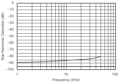
| Total harmonic distortion | VIN = 5 VP-P at 10 kHz | ADS8320E | –84 | dB | |||||
| ADS8320EB | –86 | ||||||||
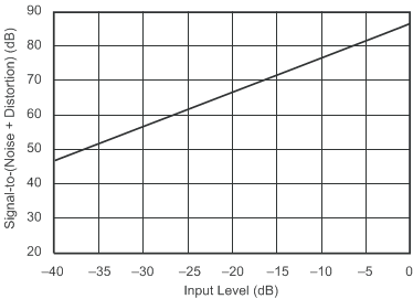
| SINAD | VIN = 5 VP-P at 10 kHz | ADS8320E | 82 | dB | |||||
| ADS8320EB | 84 | ||||||||
| Spurious-free dynamic | VIN = 5 VP-P at 10 kHz | ADS8320E | 84 | dB | |||||
| ADS8320EB | 86 | ||||||||
| SNR | ADS8320E | 90 | dB | ||||||
| ADS8320EB | 92 | ||||||||
| REFERENCE INPUT | |||||||||
| Voltage | 0.5 | VCC | V | ||||||
| Resistance | CS = GND, fSAMPLE = 0 Hz | 5 | GΩ | ||||||
| CS = VCC | 5 | ||||||||
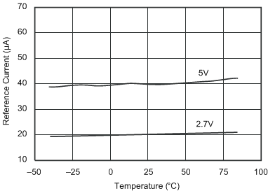
| Current drain | 40 | 80 | µA | ||||||
| fSAMPLE = 0 Hz | 0.8 | ||||||||
| CS = VCC | 0.1 | 3 | |||||||
| DIGITAL INPUT/OUTPUT | |||||||||
| Logic family | CMOS | ||||||||
| Logic levels | VIH | IIH = 5 µA | 3 | VCC + 0.3 | V | ||||
| VIL | IIL = 5 µA | –0.3 | 0.8 | ||||||
| VOH | IOH = –250 µA | 4 | |||||||
| VOL | IOL = 250 µA | 0.4 | |||||||
| Data format | Straight Binary | ||||||||
| POWER SUPPLY REQUIREMENTS | |||||||||
| VCC | Specified performance | 4.75 | 5.25 | V | |||||
| VCC(2) | 2 | 5.25 | V | ||||||
| Quiescent current | 900 | 1700 | µA | ||||||
| fSAMPLE = 10 kHz(3)(4) | 200 | ||||||||
| Power dissipation | 4.5 | 8.5 | mW | ||||||
| Power down | CS = VCC | 0.3 | 3 | µA | |||||
(1) LSB means Least Significant Bit with VREF equal to 2.5 V, one LSB is 0.038 mV.
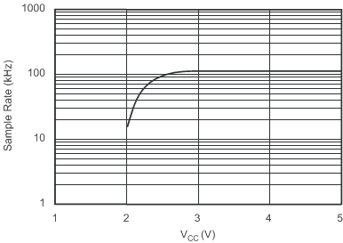
(2) See Typical Characteristics for more information.
(3) fCLK = 2.4 MHz, CS = VCC for 216 clock cycles out of every 240.
(4) See Power Dissipation for more information regarding lower sample rates.
6.6 Electrical Characteristics: VCC = 2.7 V
at –40°C to 85°C, VREF = 5 V, –IN = GND, fSAMPLE = 100 kHz, and fCLK = 24 × fSAMPLE (unless otherwise noted)| PARAMETER | TEST CONDITIONS | MIN | TYP | MAX | UNIT | |||
|---|---|---|---|---|---|---|---|---|
| RESOLUTION | ||||||||
| Resolution | 16 | Bits | ||||||
| ANALOG INPUT | ||||||||
| Full-scale input span | +In – (–In) | 0 | VREF | V | ||||
| Absolute input | +In | –0.1 | VCC + 0.1 | V | ||||
| –In | –0.1 | 0.5 | ||||||
| Capacitance | 45 | pF | ||||||
| Leakage current | 1 | nA | ||||||
| SYSTEM PERFORMANCE | ||||||||
| No missing codes | ADS8320E | 14 | Bits | |||||
| ADS8320EB | 15 | |||||||
| Integral linearity error | ADS8320E | ±0.008% | ±0.018% | FSR | ||||
| ADS8320EB | ±0.006% | ±0.012% | ||||||
| Offset error | ADS8320E | ±1 | ±2 | mV | ||||
| ADS8320EB | ±0.5 | ±1 | ||||||
| Offset temperature drift | ±3 | µV/°C | ||||||
| Gain error | ADS8320E | ±0.05% | FSR | |||||
| ADS8320EB | ±0.024% | |||||||
| Gain error temperature drift | ±0.3 | ppm/°C | ||||||
| Noise | 20 | ppm/°C | ||||||
| Power-supply rejection ratio | 2.7 V < VCC < 3.3 V | 3 | LSB(1) | |||||
| SAMPLING DYNAMICS | ||||||||
| Conversion time | 16 | Clock Cycles | ||||||
| Acquisition time | 4.5 | Clock Cycles | ||||||
| Throughput rate | 100 | kHz | ||||||
| Clock frequency | 0.024 | 2.4 | MHz | |||||
| DYNAMIC CHARACTERISTICS | ||||||||
| Total harmonic distortion | VIN = 2.7 VP-P at 1 kHz | ADS8320E | –86 | dB | ||||
| ADS8320EB | –88 | |||||||
| SINAD | VIN = 2.7 VP-P at 1 kHz | ADS8320E | 84 | dB | ||||
| ADS8320EB | 86 | |||||||
| Spurious-free dynamic | VIN = 2.7 VP-P at 1 kHz | ADS8320E | 86 | dB | ||||
| ADS8320EB | 88 | |||||||
| SNR | ADS8320E | 88 | dB | |||||
| ADS8320EB | 90 | |||||||
| REFERENCE INPUT | ||||||||
| Voltage | 0.5 | VCC | V | |||||
| Resistance | CS = GND, fSAMPLE = 0 Hz | 5 | GΩ | |||||
| CS = VCC | 5 | |||||||
| Current drain | 20 | 50 | µA | |||||
| CS = VCC | 0.1 | 3 | ||||||
| DIGITAL INPUT/OUTPUT | ||||||||
| Logic Family | CMOS | |||||||
| Logic levels | VIH | IIH = 5 µA | 2 | VCC + 0.3 | V | |||
| VIL | IIL = 5 µA | –0.3 | 0.8 | |||||
| VOH | IOH = –250 µA | 2.1 | ||||||
| VOL | IOL = 250 µA | 0.4 | ||||||
| Data format | Straight Binary | |||||||
| POWER SUPPLY REQUIREMENTS | ||||||||
| VCC | Specified performance | 2.7 | 3.3 | V | ||||
| VCC(3) | 2 | 5.25 | V | |||||
| See(2) | 2 | 2.7 | ||||||
| Quiescent current | 650 | 1300 | µA | |||||
| fSAMPLE = 10 kHz(4)(5) | 100 | |||||||
| Power dissipation | 1.8 | 3.8 | mW | |||||
| Power down | CS = VCC | 0.3 | 3 | µA | ||||
(1) LSB means Least Significant Bit with VREF equal to 2.5 V, one LSB is 0.038 mV.
(2) The maximum clock rate of the ADS8320 is less than 2.4 MHz in this power supply range.
(3) See Typical Characteristics for more information.
(4) fCLK = 2.4 MHz, CS = VCC for 216 clock cycles out of every 240.
(5) See Power Dissipation for more information regarding lower sample rates.
6.7 Typical Characteristics
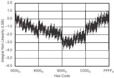
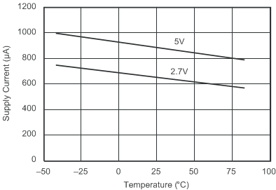
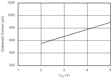
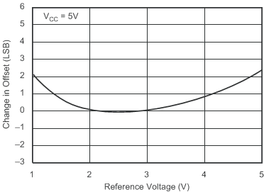
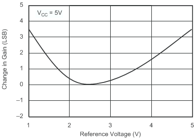
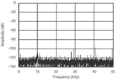
FIN = 10.120 kHz, –0.3 dB)
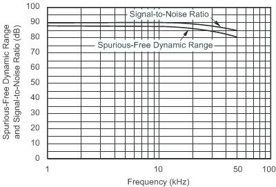
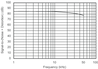
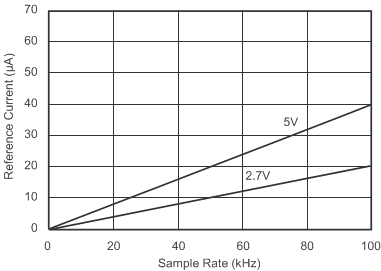
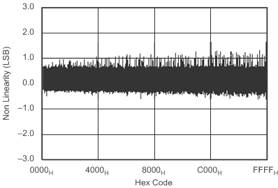
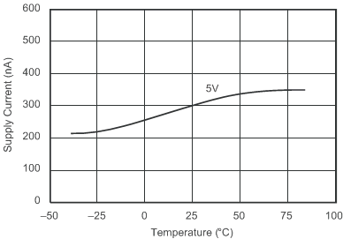
Code (25°C)
