SBAS108E May   2000  – December 2016 ADS8320

PRODUCTION DATA.  

  1. Features
  2. Applications
  3. Description
  4. Revision History
  5. Pin Configuration and Functions
  6. Specifications
    1. 6.1 Absolute Maximum Ratings
    2. 6.2 ESD Ratings
    3. 6.3 Recommended Operating Conditions
    4. 6.4 Thermal Information
    5. 6.5 Electrical Characteristics: VCC = 5 V
    6. 6.6 Electrical Characteristics: VCC = 2.7 V
    7. 6.7 Typical Characteristics
  7. Detailed Description
    1. 7.1 Overview
      1. 7.1.1 Typical Connection Diagram
    2. 7.2 Functional Block Diagram
    3. 7.3 Feature Description
      1. 7.3.1 Analog Input
      2. 7.3.2 Reference Input
      3. 7.3.3 Noise
      4. 7.3.4 Averaging
    4. 7.4 Device Functional Modes
      1. 7.4.1 Signal Levels
      2. 7.4.2 Serial Interface
      3. 7.4.3 Data Format
  8. Application and Implementation
    1. 8.1 Application Information
    2. 8.2 Typical Applications
      1. 8.2.1 Universal Sensor IF SAR Booster Pack
        1. 8.2.1.1 Design Requirements
        2. 8.2.1.2 Detailed Design Procedure
        3. 8.2.1.3 Application Curves
          1. 8.2.1.3.1 Static Test (DC)
          2. 8.2.1.3.2 Dynamic Test (AC)
      2. 8.2.2 Wireless Motor Monitor (WMM)
        1. 8.2.2.1 Design Requirements
        2. 8.2.2.2 Detailed Design Procedure
        3. 8.2.2.3 Application Curves
  9. Power Supply Recommendations
  10. 10Layout
    1. 10.1 Layout Guidelines
    2. 10.2 Layout Example
    3. 10.3 Power Dissipation
      1. 10.3.1 Short Cycling
  11. 11Device and Documentation Support
    1. 11.1 Documentation Support
      1. 11.1.1 Related Documentation
    2. 11.2 Receiving Notification of Documentation Updates
    3. 11.3 Community Resources
    4. 11.4 Trademarks
    5. 11.5 Electrostatic Discharge Caution
    6. 11.6 Glossary
  12. 12Mechanical, Packaging, and Orderable Information

封装选项

机械数据 (封装 | 引脚)
散热焊盘机械数据 (封装 | 引脚)
订购信息

Pin Configuration and Functions

DGK Package
8-Pin VSSOP
Top View
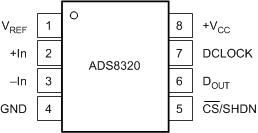
ADS8320 Pin_Config_SBAS108.gif

Pin Functions

PIN TYPE(1) DESCRIPTION
NO. NAME
1 VREF AI Reference input
2 +In AI Noninverting input
3 –In AI Inverting input: Connect to ground or to remote ground sense point.
4 GND GND Ground
5 CS/SHDN DI Chip select when LOW; Shutdown mode when HIGH.
6 DOUT DO The serial output data word is comprised of 16 bits of data. In operation the data is valid on the falling edge of DCLOCK. The second clock pulse after the falling edge of CS enables the serial output. After one null bit the data is valid for the next 16 edges.
7 DCLOCK DI Data clock synchronizes the serial data transfer and determines conversion speed.
8 +VCC PWR Power supply
AI = Analog Input, DI = Digital Input, DO = Digital Output, GND = Ground, PWR = Power