SBAS108E May 2000 – December 2016 ADS8320
PRODUCTION DATA.
- 1 Features
- 2 Applications
- 3 Description
- 4 Revision History
- 5 Pin Configuration and Functions
- 6 Specifications
- 7 Detailed Description
- 8 Application and Implementation
- 9 Power Supply Recommendations
- 10Layout
- 11Device and Documentation Support
- 12Mechanical, Packaging, and Orderable Information
7 Detailed Description
7.1 Overview
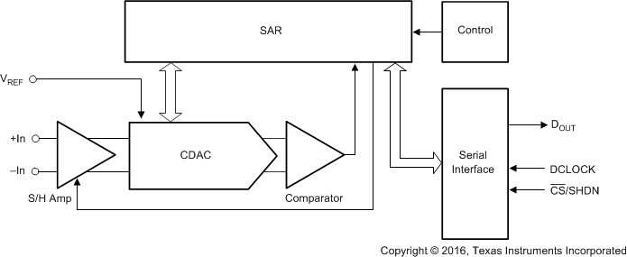
The ADS8320 device is a classic successive approximation register (SAR) analog-to-digital (A/D) converter. The architecture is based on capacitive redistribution, which inherently includes a sample and hold function. The converter is fabricated on a 0.6µm CMOS process. The architecture and process allow the ADS8320 to acquire and convert an analog signal at up to 100,000 conversions per second while consuming less than 4.5 mW from +VCC.
The ADS8320 requires an external reference, an external clock, and a single power source (VCC). The external reference can be any voltage between 500 mV and VCC. The value of the reference voltage directly sets the range of the analog input. The reference input current depends on the conversion rate of the ADS8320.
The external clock can vary between 24 kHz (1-kHz throughput) and 2.4 MHz (100-kHz throughput). The duty cycle of the clock is essentially unimportant, as long as the minimum high and low times are at least 200 ns
(VCC = 2.7 V or greater). The minimum clock frequency is set by the leakage on the capacitors internal to the ADS8320.
The analog input is provided to two input pins: +In and –In. When a conversion is initiated, the differential input on these pins is sampled on the internal capacitor array. While a conversion is in progress, both inputs are disconnected from any internal function.
The digital result of the conversion is clocked out by the DCLOCK input and is provided serially, most significant bit first, on the DOUT pin. The digital data that is provided on the DOUT pin is for the conversion currently in progress—there is no pipeline delay. It is possible to continue to clock the ADS8320 after the conversion is complete and to obtain the serial data least significant bit first. See Device Functional Modes for more information.
7.1.1 Typical Connection Diagram
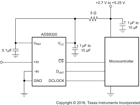
Figure 19 shows a basic data acquisition system. The ADS8320 input range is 0 V to VCC, as the reference input is connected directly to the power supply. The 5-Ω resistor and 1-µF to 10-µF capacitor filter the microcontroller noise on the supply, as well as any high-frequency noise from the supply itself. The exact values must be picked such that the filter provides adequate rejection of the noise.
 Figure 19. Typical Connection Diagram With ADS8320
7.2 Functional Block Diagram

7.3 Feature Description
7.3.1 Analog Input
The +In and –In input pins allow for a differential input signal. Unlike some converters of this type, the –In input is not resampled later in the conversion cycle. When the converter goes into the hold mode, the voltage difference between +In and –In is captured on the internal capacitor array.
The range of the –In input is limited to –0.1 V to 1 V (–0.1 V to 0.5 V when using a 2.7-V supply). Because of this, the differential input can be used to reject only small signals that are common to both inputs. Thus, the –In input is best used to sense a remote signal ground that may move slightly with respect to the local ground potential.
The input current on the analog inputs depends on a number of factors: sample rate, input voltage, source impedance, and power-down mode. Essentially, the current into the ADS8320 charges the internal capacitor array during the sample period. After this capacitance has been fully charged, there is no further input current. The source of the analog input voltage must be able to charge the input capacitance (45 pF) to a 16-bit settling level within 4.5 clock cycles. When the converter goes into the hold mode or while it is in the power down mode, the input impedance is greater than 1 GΩ.
Care must be taken regarding the absolute analog input voltage. To maintain the linearity of the converter, the –In input must not drop below GND – 100 mV or exceed GND + 1 V. The +In input must always remain within the range of GND – 100 mV to VCC + 100 mV. Outside of these ranges, the converter linearity may not meet specifications. To minimize noise, low bandwidth input signals with lowpass filters must be used.
7.3.2 Reference Input
The external reference sets the analog input range. The ADS8320 operates with a reference in the range of 500 mV to VCC. There are several important implications of this.
As the reference voltage is reduced, the analog voltage weight of each digital output code is reduced. This is often referred to as the Least Significant Bit (LSB) size and is equal to the reference voltage divided by 65,536. This means that any offset or gain error inherent in the A/D converter appears to increase, in terms of LSB size, as the reference voltage is reduced.
The noise inherent in the converter also appears to increase with lower LSB size. With a 5-V reference, the internal noise of the converter typically contributes only 1.5-LSB peak-to-peak of potential error to the output code. When the external reference is 500 mV, the potential error contribution from the internal noise is 10 times larger (15 LSBs). The errors due to the internal noise are gaussian in nature and can be reduced by averaging consecutive conversion results.
For more information regarding noise, see Figure 12. Note that the Effective Number of Bits (ENOB) figure is calculated based on the converter’s signal-to-(noise + distortion) ratio with a 1-kHz, 0-dB input signal. SINAD is related to ENOB as shown in Equation 1.
With lower reference voltages, extra care must be taken to provide a clean layout including adequate bypassing, a clean power supply, a low-noise reference, and a low-noise input signal. Because the LSB size is lower, the converter is also more sensitive to external sources of error such as nearby digital signals and electromagnetic interference.
7.3.3 Noise
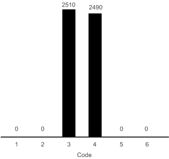
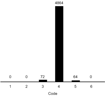
The noise floor of the ADS8320 itself is extremely low, as can be seen from Figure 20 and Figure 21, and is much lower than competing A/D converters. It was tested by applying a low-noise DC input and a 5-V reference to the ADS8320 and initiating 5000 conversions. The digital output of the A/D converter varies in output code due to the internal noise of the ADS8320. This is true for all 16-bit SAR-type A/D converters. Using a histogram to plot the output codes, the distribution must appear bell-shaped with the peak of the bell curve representing the nominal code for the input value. The ±1σ, ±2σ, and ±3σ distributions represents the 68.3%, 95.5%, and 99.7%, respectively, of all codes. The transition noise can be calculated by dividing the number of codes measured by 6 and this yields the ±3σ distribution or 99.7% of all codes. Statistically, up to 3 codes could fall outside the distribution when executing 1000 conversions. The ADS8320, with < 3 output codes for the ±3σ distribution, yields a <±0.5-LSB transition noise. Remember, to achieve this low-noise performance, the peak-to-peak noise of the input signal and reference must be < 50 µV.
 Figure 20. Histogram of 5000 Conversions of a DC Input at the Code Transition
 Figure 21. Histogram of 5000 Conversions of a DC Input at the Code Center
7.3.4 Averaging
The noise of the A/D converter can be compensated by averaging the digital codes. By averaging conversion results, transition noise is reduced by a factor of 1/√n, where n is the number of averages. For example, averaging four conversion results reduces the transition noise by 1/2 to ±0.25 LSBs. Averaging must only be used for input signals with frequencies near DC.
For AC signals, a digital filter can be used to low-pass filter and decimate the output codes. This works in a similar manner to averaging; for every decimation by 2, the signal-to-noise ratio improves 3 dB.
7.4 Device Functional Modes
7.4.1 Signal Levels
The digital inputs of the ADS8320 can accommodate logic levels up to 5.5 V regardless of the value of VCC. Thus, the ADS8320 can be powered at 3 V and still accept inputs from logic powered at 5 V.
The CMOS digital output (DOUT) swings 0 V to VCC. If VCC is 3 V and this output is connected to a 5-V CMOS logic input, then that IC may require more supply current than normal and may have a slightly longer propagation delay.
7.4.2 Serial Interface
The ADS8320 communicates with microprocessors and other digital systems through a synchronous 3-wire serial interface, as shown in Figure 3 and Table 1. The DCLOCK signal synchronizes the data transfer with each bit being transmitted on the falling edge of DCLOCK. Most receiving systems capture the bitstream on the rising edge of DCLOCK. However, if the minimum hold time for DOUT is acceptable, the system can use the falling edge of DCLOCK to capture each bit.
A falling CS signal initiates the conversion and data transfer. The first 4.5 to 5.0 clock periods of the conversion cycle are used to sample the input signal. After the fifth falling DCLOCK edge, DOUT is enabled and outputs a LOW value for one clock period. For the next 16 DCLOCK periods, DOUT outputs the conversion result, most significant bit first. After the least significant bit (B0) has been output, subsequent clocks repeat the output data but in a least significant bit first format.
After the most significant bit (B15) has been repeated, DOUT tri-states. Subsequent clocks has no effect on the converter. A new conversion is initiated only when CS has been taken HIGH and returned LOW.
Table 1. Timing Specifications (VCC = 2.7 V and Above, –40°C to 85°C)
| MIN | TYP | MAX | UNIT | ||
|---|---|---|---|---|---|
| tSMPL | Analog input sample time | 4.5 | 5 | Clock Cycles | |
| tCONV | Conversion time | 16 | Clock Cycles | ||
| tCYC | Throughput rate | 100 | kHz | ||
| tCSD | CS falling to DCLOCK LOW | 0 | ns | ||
| tSUCS | CS falling to DCLOCK rising | 20 | ns | ||
| thDO | DCLOCK falling to current DOUT not valid | 5 | 15 | ns | |
| tdDO | DCLOCK falling to next DOUT not valid | 30 | 50 | ns | |
| tdis | CS rising to DOUT Tri-state | 70 | 100 | ns | |
| ten | DCLOCK falling to DOUT | 20 | 50 | ns | |
| tf | DOUT fall time | 5 | 25 | ns | |
| tr | DOUT rise time | 7 | 25 | ns | |
7.4.3 Data Format
The output data from the ADS8320 is in straight binary format, as shown in Table 2. This table represents the ideal output code for the given input voltage and does not include the effects of offset, gain error, or noise.
Table 2. Ideal Input Voltages
| DESCRIPTION | ANALOG VALUE |
|---|---|
| Full-scale range | VREF |
| Least significant bit (LSB) | VREF/65,536 |
| Full-scale | VREF – 1 LSB |
| Midscale | VREF/2 |
| Midscale – 1 LSB | VREF/2 – 1 LSB |
| Zero | 0 V |
Table 3. Ideal Output Codes
| DIGITAL OUTPUT STRAIGHT BINARY |
|
|---|---|
| BINARY CODE | HEX CODE |
| 1111 1111 1111 1111 | FFF |
| 1000 0000 0000 0000 | 8000 |
| 0111 1111 1111 1111 | 7FFF |
| 0000 0000 0000 0000 | 0000 |