ZHCSD06 November 2014 ADS58J89
PRODUCTION DATA.
- 1 特性
- 2 应用
- 3 说明
- 4 修订历史记录
- 5 Pin Configuration and Functions
-
6 Specifications
- 6.1 Absolute Maximum Ratings
- 6.2 Handling Ratings
- 6.3 Recommended Operating Conditions
- 6.4 Thermal Information
- 6.5 Electrical Characteristics
- 6.6 Electrical Characteristics: 250 MSPS Output, 2x Decimation Filter
- 6.7 Electrical Characteristics: 500 MSPS Output
- 6.8 Electrical Characteristics: Sample Clock Timing Characteristics
- 6.9 Electrical Characteristics: Digital Outputs
- 6.10 Timing Requirements
- 6.11 Reset Timing
- 6.12 Typical Characteristics
-
7 Detailed Description
- 7.1 Overview
- 7.2 Functional Block Diagram
- 7.3
Feature Description
- 7.3.1 Decimation by 2 (250 MSPS Output)
- 7.3.2 Over-Range Indication
- 7.3.3 JESD204B Interface
- 7.3.4 SYSREF Clocking Schemes
- 7.3.5 Split-Mode Operation
- 7.3.6 Eye Diagram Information
- 7.3.7 Analog Inputs
- 7.3.8 Clock Inputs
- 7.3.9 Input Clock Divider
- 7.3.10 Power-Down Control
- 7.3.11 Device Configuration
- 7.3.12 JESD204B Interface Initialization Sequence
- 7.3.13 Device and Register Initialization
- 7.4 Device Functional Modes
- 7.5 Programming
- 7.6
Register Maps
- 7.6.1
Register Descriptions
- 7.6.1.1 Register Address 0
- 7.6.1.2 Register Address 1
- 7.6.1.3 Register Address 2
- 7.6.1.4 Register Address 3
- 7.6.1.5 Register Address 4
- 7.6.1.6 Register Address 5
- 7.6.1.7 Register Address 6
- 7.6.1.8 Register Address 7
- 7.6.1.9 Register Address 8
- 7.6.1.10 Register Address 12
- 7.6.1.11 Register Address 13
- 7.6.1.12 Register Address 14
- 7.6.1.13 Register Address 15
- 7.6.1.14 Register Address 16
- 7.6.1.15 Register Address 19
- 7.6.1.16 Register Address 22
- 7.6.1.17 Register Address 23
- 7.6.1.18 Register Address 26
- 7.6.1.19 Register Address 29
- 7.6.1.20 Register Address 30
- 7.6.1.21 Register Address 31
- 7.6.1.22 Register Address 32
- 7.6.1.23 Register Address 33
- 7.6.1.24 Address: 0x24, 0x25, 0x26, 0x27
- 7.6.1.25 Address: 0x28, 0x29, 0x2A, 0x2B
- 7.6.1.26 Register Address 44
- 7.6.1.27 Register Address 45
- 7.6.1.28 Register Address 46
- 7.6.1.29 Register Address 47
- 7.6.1.30 Address: 0x32, 0x33, 0x34, 0x35
- 7.6.1.31 Address: 0x36, 0x37, 0x38, 0x39
- 7.6.1.32 Register Address 58
- 7.6.1.33 Register Address 59
- 7.6.1.34 Register Address 60
- 7.6.1.35 Register Address 61
- 7.6.1.36 Register Address 99
- 7.6.1.37 Register Address 100
- 7.6.1.38 Register Address 103
- 7.6.1.39 Register Address 104
- 7.6.1.40 Register Address 107
- 7.6.1.41 Register Address 108
- 7.6.1.42 Register Address 111
- 7.6.1
Register Descriptions
- 8 Application and Implementation
- 9 Power Supply Recommendations
- 10Layout
- 11器件和文档支持
- 12机械封装和可订购信息
8 Application and Implementation
NOTE
Information in the following applications sections is not part of the TI component specification, and TI does not warrant its accuracy or completeness. TI’s customers are responsible for determining suitability of components for their purposes. Customers should validate and test their design implementation to confirm system functionality.
8.1 Application Information
In the design of any application involving a high-speed data converter, particular attention should be paid the design of the analog input, the clocking solution, and careful layout of the clock and analog signals. In addition, the JESD204B interface means there now are high-speed serial lines that should be handled to preserve adequate signal integrity at the device that receives the sample data. The ADS58J89 evaluation module (EVM) is one practical example of the design of the analog input circuit and clocking solution, as well as a practical example of good circuit board layout practices around the ADC.
8.1.1 SNR and Clock Jitter
The signal-to-noise ratio of the channel is limited by three different factors: the quantization noise is typically not noticeable in pipeline converters and is 84 dB for a 14-bit channel. The thermal noise limits the SNR at low input frequencies while the clock jitter sets the SNR for higher input frequencies.
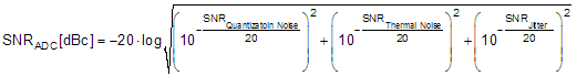
Calculate the SNR limitation due to sample clock jitter using the following:

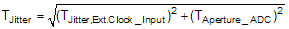
The total clock jitter (tJitter) has two components – the internal aperture jitter (85 fs for ADS58J89), which is set by the noise of the clock input buffer, the external clock jitter, and the jitter from the analog input signal. Calculate total clock jitter using the following:
External clock jitter can be minimized by using high quality clock sources and jitter cleaners, as well as bandpass filters at the clock input while a faster clock slew rate improves the channel aperture jitter.
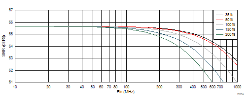
The ADS58J89 has a thermal noise of 66 dBFS and internal aperture jitter of 98 fs. The SNR depending on amount of external jitter for different input frequencies is shown in Figure 107.
8.2 Typical Application
The analog inputs of the ADS58J89 must be fully differential and biased to a desired common mode voltage, VCM. Therefore, there will be a signal conditioning circuit for each of the analog inputs. If the amplitude of the input circuit is such that no gain is needed to make full use of the full-scale range of the ADC, then a transformer coupled circuit as in Figure 108 may be used with good results. The transformer coupling is inherently low-noise, and inherently AC-coupled so that the signal may be biased to VCM after the transformer coupling. If signal gain is required, or the input bandwidth is to include the spectrum all the way down to DC such that AC coupling is not possible, then an amplifier-based signal conditioning circuit would be required.
By using the simple drive circuit of Figure 108, uniform performance can be obtained over a wide frequency range. The buffers present at the analog inputs of the device help isolate the external drive source from the switching currents of the sampling circuit.
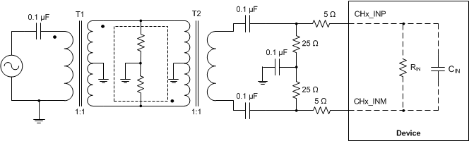 Figure 108. Input Drive Circuit
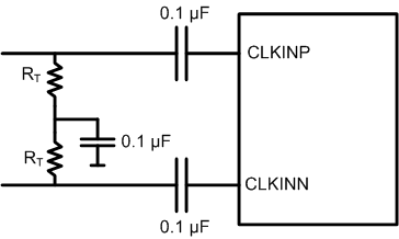 Figure 109. Recommended Differential Clock Driving Circuit
8.2.1 Design Requirements
The ADS58J89 requires a fully differential analog input with a full-scale range not to exceed 1.25 V peak to peak, biased to a common mode voltage of 2.0 V. In addition the input circuit must provide proper transmission line termination (or proper load resistors in an amplifier-based solution) so the input of the impedance of the ADC analog inputs should be considered as well.
The clocking solution will have a direct impact on performance in terms of SNR, as shown in Figure 107. The ADS58J89 is capable of a typical SNR of 66 dBFS for input frequencies of about 100 MHz (in 14-bit burst mode), so we will want to have a clocking solution that can preserve this level of performance.
8.2.2 Detailed Design Procedure
The ADS58J89 has an input bandwidth of approximately 900 MHz, but we will consider an application involving the first or second Nyquist zones, so we will limit the frequency bandwidth here to be under 250 MHz. We will also consider a 50-ohm signal source, so the proper termination would be 50-Ω differential. As seen in Figure 110 and Figure 111, the input impedance of the analog input at 250 MHz is large compared to 50 Ω, so the proper termination can be 50-Ω differential as shown in Figure 108. Splitting the termination into two 25-Ω resistors with an AC capacitor to ground provides a path to filter out any ripple on the common mode that may result from any amplitude or phase imbalance of the differential input, improving SFDR performance. The ADS58J89 provides a VCM output that may be used to bias the input to the desired level, but as seen in Figure 52 the signal is internally biased inside the ADC so an external biasing to VCM is not required. If an external biasing to VCM were to be employed, the VCM voltage may be applied to the mid-point of the two 25-Ω termination resistors in Figure 108.
For the clock input, Figure 107 shows the SNR of the device above 100 MHz begins to degrade with external clock jitter of greater than 100 fs rms, so we will recommend the clock source be limited to approximately 100 fS of rms jitter. For the ADS58J89 EVM, the LMK04828 clock device is capable of providing a low-jitter sample clock as well as providing the SYSREF signal required as shown in Figure 47 and Figure 48, so that clocking device is one good choice for the clocking solution for the ADS58J89.
8.2.3 Application Curves
Figure 110 and Figure 111 show the differential impedance between the channel INP and INM pins. The impedance is modeled as a parallel combination of RIN and CIN (RIN || 1 / jwCIN).
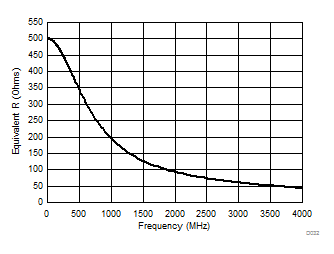 Figure 110. Equivalent R
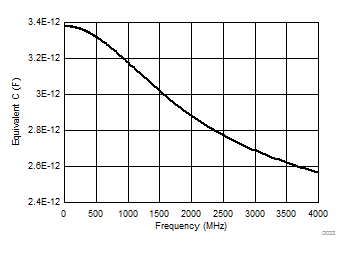 Figure 111. Equivalent C