ZHCSD06 November 2014 ADS58J89
PRODUCTION DATA.
- 1 特性
- 2 应用
- 3 说明
- 4 修订历史记录
- 5 Pin Configuration and Functions
-
6 Specifications
- 6.1 Absolute Maximum Ratings
- 6.2 Handling Ratings
- 6.3 Recommended Operating Conditions
- 6.4 Thermal Information
- 6.5 Electrical Characteristics
- 6.6 Electrical Characteristics: 250 MSPS Output, 2x Decimation Filter
- 6.7 Electrical Characteristics: 500 MSPS Output
- 6.8 Electrical Characteristics: Sample Clock Timing Characteristics
- 6.9 Electrical Characteristics: Digital Outputs
- 6.10 Timing Requirements
- 6.11 Reset Timing
- 6.12 Typical Characteristics
-
7 Detailed Description
- 7.1 Overview
- 7.2 Functional Block Diagram
- 7.3
Feature Description
- 7.3.1 Decimation by 2 (250 MSPS Output)
- 7.3.2 Over-Range Indication
- 7.3.3 JESD204B Interface
- 7.3.4 SYSREF Clocking Schemes
- 7.3.5 Split-Mode Operation
- 7.3.6 Eye Diagram Information
- 7.3.7 Analog Inputs
- 7.3.8 Clock Inputs
- 7.3.9 Input Clock Divider
- 7.3.10 Power-Down Control
- 7.3.11 Device Configuration
- 7.3.12 JESD204B Interface Initialization Sequence
- 7.3.13 Device and Register Initialization
- 7.4 Device Functional Modes
- 7.5 Programming
- 7.6
Register Maps
- 7.6.1
Register Descriptions
- 7.6.1.1 Register Address 0
- 7.6.1.2 Register Address 1
- 7.6.1.3 Register Address 2
- 7.6.1.4 Register Address 3
- 7.6.1.5 Register Address 4
- 7.6.1.6 Register Address 5
- 7.6.1.7 Register Address 6
- 7.6.1.8 Register Address 7
- 7.6.1.9 Register Address 8
- 7.6.1.10 Register Address 12
- 7.6.1.11 Register Address 13
- 7.6.1.12 Register Address 14
- 7.6.1.13 Register Address 15
- 7.6.1.14 Register Address 16
- 7.6.1.15 Register Address 19
- 7.6.1.16 Register Address 22
- 7.6.1.17 Register Address 23
- 7.6.1.18 Register Address 26
- 7.6.1.19 Register Address 29
- 7.6.1.20 Register Address 30
- 7.6.1.21 Register Address 31
- 7.6.1.22 Register Address 32
- 7.6.1.23 Register Address 33
- 7.6.1.24 Address: 0x24, 0x25, 0x26, 0x27
- 7.6.1.25 Address: 0x28, 0x29, 0x2A, 0x2B
- 7.6.1.26 Register Address 44
- 7.6.1.27 Register Address 45
- 7.6.1.28 Register Address 46
- 7.6.1.29 Register Address 47
- 7.6.1.30 Address: 0x32, 0x33, 0x34, 0x35
- 7.6.1.31 Address: 0x36, 0x37, 0x38, 0x39
- 7.6.1.32 Register Address 58
- 7.6.1.33 Register Address 59
- 7.6.1.34 Register Address 60
- 7.6.1.35 Register Address 61
- 7.6.1.36 Register Address 99
- 7.6.1.37 Register Address 100
- 7.6.1.38 Register Address 103
- 7.6.1.39 Register Address 104
- 7.6.1.40 Register Address 107
- 7.6.1.41 Register Address 108
- 7.6.1.42 Register Address 111
- 7.6.1
Register Descriptions
- 8 Application and Implementation
- 9 Power Supply Recommendations
- 10Layout
- 11器件和文档支持
- 12机械封装和可订购信息
10 Layout
10.1 Layout Guidelines
The Device EVM layout can be used as a reference layout to obtain the best performance. A layout diagram of the EVM top layer is provided in . Some important points to remember during laying out the board are:
- Analog inputs are located on opposite sides of the device pinout to ensure minimum crosstalk on the package level. To minimize crosstalk on-board, the analog inputs should exit the pinout in opposite directions, as shown in the reference layout of as much as possible.
- In the device pinout, the sampling clock is located on a side perpendicular to the analog inputs in order to minimize coupling between them. This configuration is also maintained on the reference layout of as much as possible.
- Digital outputs should be kept away from the analog inputs. When these digital outputs exit the pinout, the digital output traces should not be kept parallel to the analog input traces because this configuration may result in coupling from digital outputs to analog inputs and degrade performance. The digital sample data rate can be as high as 5.0 Gsps, so care must be taken to maintain the signal integrity of these signals. A low-loss dielectric circuit board is recommended or else these traces should be kept as short as possible. These traces should be kept away from the analog inputs ad n clock input to the device as well.
- At each power-supply pin (AVDD, DRVDD, or AVDDD3V), a 0.1-μF decoupling capacitor should be kept close to the device. A separate decoupling capacitor group consisting of a parallel combination of 10-μF,
1-μF, and 0.1-μF capacitors can be kept close to the supply source.
10.1.1 CML SerDes Transmitter Interface
Each of the 5 Gbps SerDes CML transmitter outputs requires AC coupling between transmitter and receiver. The differential pair should be terminated with a 100-Ω resistor as close to the receiving device as possible to avoid unwanted reflections and signal degradation.
10.2 Layout Example
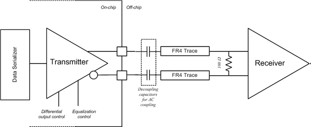 Figure 112. Layout Example Schematic
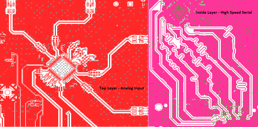 Figure 113. Top and Bottom Layers