ZHCSD06 November 2014 ADS58J89
PRODUCTION DATA.
- 1 特性
- 2 应用
- 3 说明
- 4 修订历史记录
- 5 Pin Configuration and Functions
-
6 Specifications
- 6.1 Absolute Maximum Ratings
- 6.2 Handling Ratings
- 6.3 Recommended Operating Conditions
- 6.4 Thermal Information
- 6.5 Electrical Characteristics
- 6.6 Electrical Characteristics: 250 MSPS Output, 2x Decimation Filter
- 6.7 Electrical Characteristics: 500 MSPS Output
- 6.8 Electrical Characteristics: Sample Clock Timing Characteristics
- 6.9 Electrical Characteristics: Digital Outputs
- 6.10 Timing Requirements
- 6.11 Reset Timing
- 6.12 Typical Characteristics
-
7 Detailed Description
- 7.1 Overview
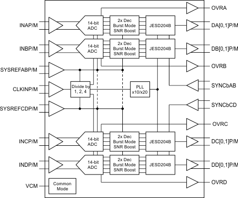
- 7.2 Functional Block Diagram
- 7.3
Feature Description
- 7.3.1 Decimation by 2 (250 MSPS Output)
- 7.3.2 Over-Range Indication
- 7.3.3 JESD204B Interface
- 7.3.4 SYSREF Clocking Schemes
- 7.3.5 Split-Mode Operation
- 7.3.6 Eye Diagram Information
- 7.3.7 Analog Inputs
- 7.3.8 Clock Inputs
- 7.3.9 Input Clock Divider
- 7.3.10 Power-Down Control
- 7.3.11 Device Configuration
- 7.3.12 JESD204B Interface Initialization Sequence
- 7.3.13 Device and Register Initialization
- 7.4 Device Functional Modes
- 7.5 Programming
- 7.6
Register Maps
- 7.6.1
Register Descriptions
- 7.6.1.1 Register Address 0
- 7.6.1.2 Register Address 1
- 7.6.1.3 Register Address 2
- 7.6.1.4 Register Address 3
- 7.6.1.5 Register Address 4
- 7.6.1.6 Register Address 5
- 7.6.1.7 Register Address 6
- 7.6.1.8 Register Address 7
- 7.6.1.9 Register Address 8
- 7.6.1.10 Register Address 12
- 7.6.1.11 Register Address 13
- 7.6.1.12 Register Address 14
- 7.6.1.13 Register Address 15
- 7.6.1.14 Register Address 16
- 7.6.1.15 Register Address 19
- 7.6.1.16 Register Address 22
- 7.6.1.17 Register Address 23
- 7.6.1.18 Register Address 26
- 7.6.1.19 Register Address 29
- 7.6.1.20 Register Address 30
- 7.6.1.21 Register Address 31
- 7.6.1.22 Register Address 32
- 7.6.1.23 Register Address 33
- 7.6.1.24 Address: 0x24, 0x25, 0x26, 0x27
- 7.6.1.25 Address: 0x28, 0x29, 0x2A, 0x2B
- 7.6.1.26 Register Address 44
- 7.6.1.27 Register Address 45
- 7.6.1.28 Register Address 46
- 7.6.1.29 Register Address 47
- 7.6.1.30 Address: 0x32, 0x33, 0x34, 0x35
- 7.6.1.31 Address: 0x36, 0x37, 0x38, 0x39
- 7.6.1.32 Register Address 58
- 7.6.1.33 Register Address 59
- 7.6.1.34 Register Address 60
- 7.6.1.35 Register Address 61
- 7.6.1.36 Register Address 99
- 7.6.1.37 Register Address 100
- 7.6.1.38 Register Address 103
- 7.6.1.39 Register Address 104
- 7.6.1.40 Register Address 107
- 7.6.1.41 Register Address 108
- 7.6.1.42 Register Address 111
- 7.6.1
Register Descriptions
- 8 Application and Implementation
- 9 Power Supply Recommendations
- 10Layout
- 11器件和文档支持
- 12机械封装和可订购信息
1 特性
- 4 通道、14 位 500MSPS,具有数字信号处理功能
- 功率放大器线性化(反馈)模式
- 14 位 250MSPS 间隔采样
- 可编程分辨率与占空比
- 占空比 3:2(60% 11 位,40% 9 位)
- 占空比 2:3(40% 12 位,60% 9 位)
- 占空比 1:3(25% 14 位,75% 9 位)
- 流量接收器模式
- 14 位 250MSPS:2 倍抽取率滤波器,高通/低通
- 9 位滤波器信噪比 (SNR) 提升模式(最大带宽为 150MHz)
- 9 至 14 位时分双工 (TDD) 突发模式(最大带宽为 200MHz)
- 灵活的输入时钟缓冲器,支持 1/2/4 分频
- JESD204B 数字接口(速率高达 5.0Gbps)
- 每个通道有 1 或 2 个信道,支持子类 1
- 64 引脚超薄型四方扁平无引线 (VQFN) 封装 (9mm × 9mm)
2 应用
- 多载波、多模式、多频带蜂窝接收器
- TDD-LTE
- FDD-LTE
- CDMA、WCMDA、CMDA2k
- GSM
- 射频 (RF) 和微波回程
- 点对点回程
- 点对多点回程
- 无线中继器
- 分布式天线系统 (DAS)
- 无线宽带
3 说明
ADS58J89 是一款高线性度、四通道、14 位 250/500MSPS IF(中频)接收器。 四个通道上均有 14 位 500MSPS 模数转换器 (ADC),用于处理无线基础设施系统的信号。 各通道可根据带宽、分辨率和采样时间要求配置为不同模式。 信号处理模块包含可选模式:抽取滤波器模式、滤波器 SNR 提升模式、分辨率与时间模式以及时分双工 (TDD) 突发模式。 这 4 个通道针对多天线系统进行设计,为采用小型封装的多通道接收器提供了较高的带宽与线性度。 在 TDD 系统中,此器件可同时用作流量接收器和功率放大器线性化反馈路径。
主要技术规格:
- 功耗:每通道 875mW
- 输入带宽 (3dB):900MHz
- 孔径抖动:98fs rms
- 通道隔离:85dB
- ƒin = 170MHz(–1dBFS,–1dBFS)
条件下的性能- SNR:65.8dBFS
- 无杂散动态范围 (SFDR):85dBc(HD2,HD3);95dBFS(非 HD2,HD3)
器件信息(1)
| 部件号 | 封装 | 最大输出速率 |
|---|---|---|
| ADS58J89 | VQFN (64) | 500MSPS |
- 要了解所有可用封装,请见数据表末尾的可订购产品附录。
简化电路原理图
4 修订历史记录
| 日期 | 修订版本 | 注释 |
|---|---|---|
| 2014 年 11 月 | * | 最初发布。 |