ZHCS190D May 2011 – November 2015 ADS5263
PRODUCTION DATA.
- 1 特性
- 2 应用
- 3 说明
- 4 修订历史记录
- 5 说明 (续)
- 6 Pin Configuration and Functions
-
7 Specifications
- 7.1 Absolute Maximum Ratings
- 7.2 ESD Ratings
- 7.3 Recommended Operating Conditions
- 7.4 Thermal Information
- 7.5 Electrical Characteristics, Dynamic Performance - 16-Bit ADC
- 7.6 Electrical Characteristics, General - 16-Bit ADC Mode
- 7.7 Electrical Characteristics, Dynamic Performance - 14-Bit ADC
- 7.8 Digital Characteristics
- 7.9 Timing Requirements
- 7.10 LVDS Timing at Lower Sampling Frequencies - 2 Wire, 8× Serialization
- 7.11 LVDS Timing for 1 Wire 16× Serialization
- 7.12 LVDS Timing for 2 Wire, 7× Serialization
- 7.13 LVDS Timing for 1 Wire, 14× Serialization
- 7.14 Serial Interface Timing Requirements
- 7.15 Reset Switching Characteristics
- 7.16 Typical Characteristics
-
8 Detailed Description
- 8.1 Overview
- 8.2 Functional Block Diagram
- 8.3 Feature Description
- 8.4 Device Functional Modes
- 8.5 Programming
- 8.6 Register Maps
- 9 Application and Implementation
- 10Power Supply Recommendations
- 11Layout
- 12器件和文档支持
- 13机械、封装和可订购信息
8 Detailed Description
8.1 Overview
The ADS5263 is a high-SNR 16-bit, quad-channel, 100-MSPS ADC using serial LVDS interface to reduce pin connections from ADC to FPGA. For low power applications, the part can be progammed into 14-bit, Low-power mode saving 615 m-W at 100-MSPS
The ADS5263 has a digital processing block that integrates several commonly used digital functions, such as digital gain (up to 12 dB). It includes a digital filter module that has built-in decimation filters (with low-pass, high-pass and band-pass characteristics). The decimation rate is also programmable (by 2, by 4, or by 8). This makes it very useful for narrow-band applications, where the filters can be used to improve SNR and knock-off harmonics, while at the same time reducing the output data rate.
The device includes an averaging mode where two channels (or even four channels) can be averaged to improve SNR. A very unique feature is the programmable mapper module that allows flexible mapping between the input channels and the LVDS output pins. This helps to greatly reduce the complexity of LVDS output routing and can potentially result in cheaper system boards by reducing the number of PCB layers.
The data from each channel ADC is serialized and output on two pairs of LVDS output lines, along with a bit clock and a frame clock. Serial LVDS outputs reduce the number of interface lines. This, together with the low-power design, enables four channels to be packaged in a compact 9-mm × 9-mm QFN, allowing high system integration densities.
In order to ease interfacing to CCD sensors, a clamp function is integrated in the device. Using this feature, the analog input pins can be clamped to an internal voltage, based on a SYNC signal. With this, the CCD sensor output can be easily ac-coupled to the ADS5263 analog inputs. The clamp feature and quad channels in a compact package make the ADS5263 attractive for industrial CCD imaging applications.
The device integrates an internal reference trimmed to accurately match across devices. Additionally, the device supports an external reference mode for applications that require very low temperature drift of reference. The ADS5263 is available in a non-magnetic QFN package that does not create any MRI signature. The device is specified over the full industrial temperature range.
8.2 Functional Block Diagram
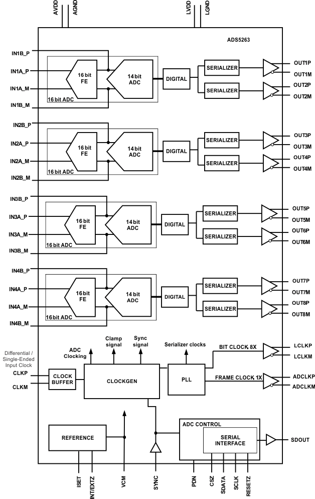 Figure 44. ADS5263 Block Diagram
8.3 Feature Description
8.3.1 Digital Processing Blocks
The ADS5263 integrates a set of commonly useful digital functions that can be used to ease system design. These functions are shown in the digital block diagram of Figure 45 and described in the following sections.
 Figure 45. Block Diagram – Digital Processing
8.3.2 Digital Gain
ADS5263 includes programmable digital gain settings from 0 dB to 12 dB in steps of 1 dB. The benefit of digital gain is to get improved SFDR performance. The SFDR improvement is achieved at the expense of SNR; for each gain setting, the SNR degrades by about 1 dB. So, the gain can be used to trade off between SFDR and SNR.
For each gain setting, the analog supported input full-scale range scales proportionally, as shown in Table 1. The full-scale range depends on the ADC mode used (16-bit or 14-bit).
After a reset, the device comes up in the 0-dB gain mode. To use other gain settings, program the <GAIN CH x> register bits.
Table 1. Analog Full-Scale Range Across Gains
| DIGITAL GAIN, dB |
16-BIT ADC MODE | 14-BIT ADC MODE |
|---|---|---|
| ANALOG FULL-SCALE INPUT, Vpp | ANALOG FULL-SCALE INPUT, Vpp | |
| 0 | 4.00 | 2 |
| 1 | 3.57 | 1.78 |
| 2 | 3.18 | 1.59 |
| 3 | 2.83 | 1.42 |
| 4 | 2.52 | 1.26 |
| 5 | 2.25 | 1.12 |
| 6 | 2.00 | 1.00 |
| 7 | 1.79 | 0.89 |
| 8 | 1.59 | 0.80 |
| 9 | 1.42 | 0.71 |
| 10 | 1.26 | 0.63 |
| 11 | 1.13 | 0.56 |
| 12 | 1.00 | 0.50 |
8.3.3 Digital Filter
The digital processing block includes the option to filter and decimate the ADC data outputs digitally. Various filters and decimation rates are supported – decimation rates of 2, 4, and 8 and low-pass, high-pass, and band-pass filters are available. The filters are internally implemented as a 24-tap asymmetric FIR (even-tap) using pre-defined coefficients following the equation which is described in Figure 46.
Alternatively, some of the filters can be configured as a 23-tap asymmetric FIR (or odd-tap filters) following the equation which is described in Figure 47.
 Figure 46. 24-tap Filter Equation
 Figure 47. 23-tap Filter Equation
In the equations,
h0, h1 …h11 are 12-bit signed 2s complement representation of the coefficients (-2048 to +2047)
x(n) is the input data sequence to the filter
y(n) is the filter output sequence
Details of the registers used for configuring the digital filters are show in Table 2 and Table 3.
Table 2. Digital Filter Registers
| BIT | NAME | DESCRIPTION |
|---|---|---|
| ADDR: 2E, 2F, 30, 31 Default = 0 | ||
| D9-D7 | FILTER TYPE CHn<2:0> | Selects low-pass, high-pass or band-pass filters |
| D6-D4 | DEC by RATE CHn<2:0> | Selects the decimation rate |
| D2 | ODD TAP CHn | Even tap or odd tap |
| D0 | USE FILTER CHn | Enables the filter |
| ADDR: 38, Default = 0 | ||
| D1-D0 | OUTPUT RATE<1:0> | Select output data rate depending on the type of filter |
| ADDR: 29, Default = 0 | ||
| D1 | EN DIG FILTER | Enables digital filter – global control |
See Table 3 for choosing the right combination of decimation rate and filter types.
Table 3. Digital Filters
| DECIMATION | TYPE OF FILTER | <OUTPUT RATE> | DEC by RATE CHx> | <FILTER TYPE CHx> | <SEL ODD TAP> | <USE FILTER CHx> | <EN CUSTOM FILT> | <EN DIG FILTER> |
|---|---|---|---|---|---|---|---|---|
| Decimate by 2 | Built-in low-pass odd-tap filter (pass band = 0 to fS/4) | 001 | 000 | 000 | 1 | 1 | 0 | 1 |
| Built-in high-pass odd-tap filter (pass band = 0 to fS/4) | 001 | 000 | 001 | 1 | 1 | 0 | 1 | |
| Decimate by 4 | Built-in low-pass even-tap filter (pass band = 0 to fS/8) | 010 | 001 | 010 | 0 | 1 | 0 | 1 |
| Built-in first band pass even tap filter(pass band = fS/8 to fS/4) | 010 | 001 | 011 | 0 | 1 | 0 | 1 | |
| Built-in second band pass even tap filter(pass band = fS/4 to 3 fS/8) | 010 | 001 | 100 | 0 | 1 | 0 | 1 | |
| Built-in high pass odd tap filter (pass band = 3 fS/8 to fS/2) | 010 | 001 | 101 | 1 | 1 | 0 | 1 | |
| Decimate by 2 | Custom filter (user programmablecoefficients) | 001 | 000 | 000 | 0 or 1 | 1 | 1 | 1 |
| Decimate by 4 | Custom filter (user programmablecoefficients) | 010 | 001 | 000 | 0 or 1 | 1 | 1 | 1 |
| Decimate by 8 | Custom filter (user programmablecoefficients) | 011 | 100 | 000 | 0 or 1 | 1 | 1 | 1 |
| 12-tap filter without decimation | Custom filter (user programmablecoefficients) | 000 | 011 | 000 | 0 | 1 | 1 | 1 |
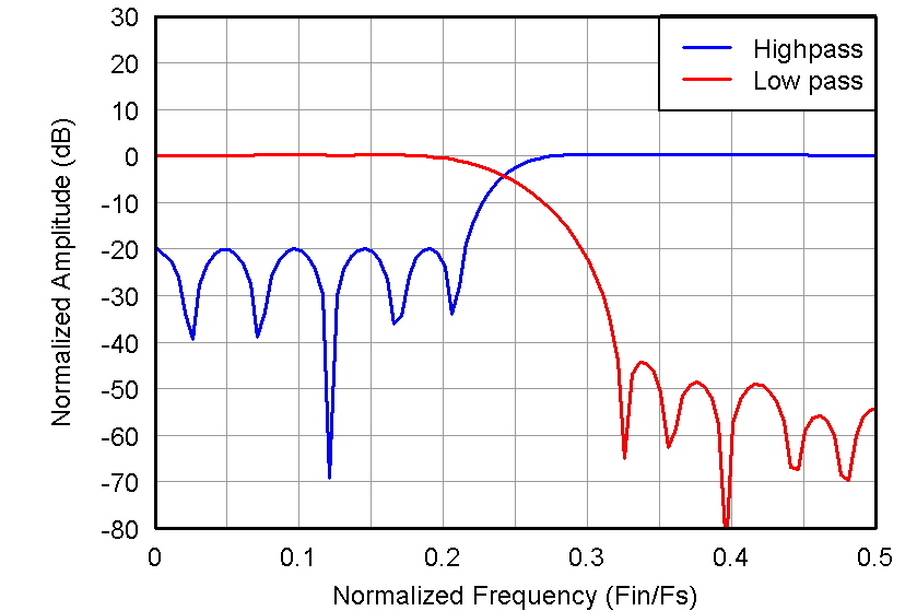 Figure 48. Filter Response – Decimate by 2
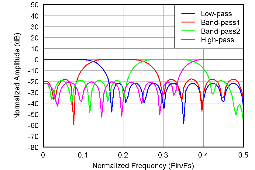 Figure 49. Filter Response – Decimate by 4
8.3.4 Custom Filter Coefficients
In addition to these built-in filters, customers also have the option of using their own custom 12-bit signed coefficients. Only 12 coefficients can be specified according to Figure 48 or Figure 49. These coefficients (h0 to h11) must be configured in the custom coefficient registers as:
Register content = 12-bit signed representation of [real coefficient value × 211]
The 12 custom coefficients must be loaded into 12 separate registers for each channel (refer Table 4 ). The MSB bit of each coefficient register decides if the built in filters or custom filters are used. If the MSB bit <EN CUSTOM FILT> is reset to 0, then built in filter coefficients are used. Else, the custom coefficients are used.
Table 4. Custom Coefficient Registers (1)
| BIT | NAME | DESCRIPTION |
|---|---|---|
| ADDR: 5A to 65, Default = 0 Set value of h0 in register 0x5A, h1 in 0x5B & so on till h11 in register 0x65 |
||
| D11-D0 | COEFFn SET CH1<11:0> | Custom coefficient for digital filter of channel 1 |
| D15 | <EN CUSTOM FILT CH1> | 1: Enables custom coefficients to be used 0: Built in coefficients are used |
| ADDR: 66 to 71, Default = 0 Set value of h0 in register 0x66, h1 in 0x67 & so on till h11 in register 0x71 |
||
| D11-D0 | COEFFn SET CH2<11:0> | Custom coefficient for digital filter of channel 2 |
| D15 | <EN CUSTOM FILT CH2> | 1: Enables custom coefficients to be used 0: Built in coefficients are used |
| ADDR: 72 to 7D, Default = 0 Set value of h0 in register 0x72, h1 in 0x73 & so on till h11 in register 0x7D |
||
| D11-D0 | COEFFn SET CH3<11:0> | Custom coefficient for digital filter of channel 3 |
| D15 | <EN CUSTOM FILT CH3> | 1: Enables custom coefficients to be used 0: Built in coefficients are used |
| ADDR: 7E to 89, Default = 0 Set value of h0 in register 0x7E, h1 in 0x7F & so on till h11 in register 0x89 |
||
| D11-D0 | COEFFn SET CH4<11:0> | Custom coefficient for digital filter of channel 4 |
| D15 | <EN CUSTOM FILT CH4> | 1: Enables custom coefficients to be used 0: Built in coefficients are used |
8.3.4.1 Custom Filter Without Decimation
Another mode exists to use the digital filter without decimation. In this mode, the filter behaves like a 12-tap symmetric FIR filter as per the equation described by Figure 50
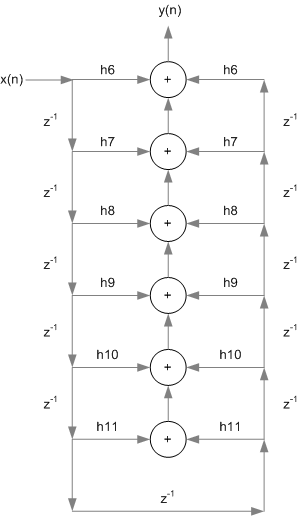 Figure 50. 12-tap Symmetric Filter Equation
Where,
h6, h7 …h11 are 12-bit signed 2s complement representation of the coefficients (-2048 to +2047)
x(n) is the input data sequence to the filter
y(n) is the filter output sequence
In this mode, as the filter is implemented as a 12-tap symmetric FIR, only 6 custom coefficients need to be specified and must be loaded in registers h6 to h11. Table 4
To enable this mode, use the register setting specified in the last row of Table 3
8.3.5 Digital Averaging
The ADS5263 includes an averaging function where the ADC digital data from two (or four) channels can be averaged. The averaged data is output on specific LVDS channels. Table 5 shows the combinations of the input channels that can be averaged and the LVDS channels on which averaged data is available
Table 5. Using Channel Averaging
| Averaged Channels | Output on Which Averaged Data Is Available | Register Settings |
|---|---|---|
| Channel 1, Channel 2 | OUT1A, OUT1B | Set <AVG OUT 1> = 10 and <EN AVG GLO> = 1 |
| Channel 1, Channel 2 | OUT3A, OUT3B | Set <AVG OUT 3> = 11 and <EN AVG GLO> = 1 |
| Channel 3, Channel 4 | OUT4A, OUT4B | Set <AVG OUT 4> = 10 and <EN AVG GLO> = 1 |
| Channel 3, Channel 4 | OUT2A, OUT2B | Set <AVG OUT 2> = 11 and <EN AVG GLO> = 1 |
| Channel 1, Channel 2, Channel 3, Channel 4 | OUT1A, OUT1B | Set <AVG OUT 1> = 11 and <EN AVG GLO> = 1 |
| Channel 1, Channel 2, Channel 3, Channel 4 | OUT1A, OUT1B | Set <AVG OUT 4> = 11 and <EN AVG GLO> = 1 |
8.3.6 Performance with Digital Processing Blocks
The ADS5263 provides very high SNR along with high sampling rates. In applications where even higher SNR performance is desired, digital processing blocks such as averaging and decimation filters can be used advantageously to achieve this. Table 6 shows the improvement in SNR that can be achieved compared to the default value, using these modes.
Table 6. SNR Improvement Using Digital Processing (1)
| MODE | TYPICAL SNR, dBFS | TYPICAL IMPROVEMENT in SNR, dB |
|---|---|---|
| Default | 84.5 | |
| With decimation-by-2 filter enabled | 86.7 | 2.2 |
| With decimation-by-4 filter enabled | 87.7 | 3.2 |
| With decimation-by-8 filter enabled | 88.6 | 4.1 |
| With two channels averaged and decimation-by-8 filter enabled | 91.3 | 6.8 |
| With four channels averaged | 89.6 | 5.1 |
| With four channels averaged and decimation-by-8 filter enabled | 93 | 8.5 |
8.3.6.1 18-Bit Data Output with Digital Processing
As shown in Table 6, very high SNR can be achieved using the digital blocks. Now, the overall SNR is limited by the quantization noise of the 16-bit output data. (16-bit quantization SNR = 6n + 1.76 = 16 × 6 + 1.76 = 97.76 dBFS.) To overcome this, the digital processing blocks (averaging and digital filters) automatically output 18-bit data. With the two additional bits, the quantization SNR improves by 12 dB and no longer limits the maximum SNR that can be achieved using the ADS5263. For example, with four channels averaged and the decimation-by-8 filter, the typical SNR improves to about 94.5 dBFS using 18-bit data (an improvement of 1.5 dB over the SNR with 16-bit data).
The 18-bit data can be output using the special 18× serialization mode (see Output LVDS Interface). Note that the user can choose either the default 16× serialization (which takes the upper 16 bits of the 18-bit data) or the 18× serialization mode (that outputs all 18 bits).
8.3.7 Flexible Mapping o Channel Data to LVDS Outputs
ADS5263 has a mapping function by the use of which the digital data for any channel can be routed to any LVDS output. So, as an example, in the 1-wire interface, the channel-1 ADC output can be output either on OUT1 pins or on OUT2 or OUT3 or OUT4 pins.
This flexibility in mapping simplifies board designs by avoiding complex routing that would be caused by a rigid mapping of input channels and output pins. This can also lead to potential saving in PCB layers and hence cost. The mapping is programmable using the register bits <MAP_Ch1234_OUTn> as shown in Figure 51 and Figure 52.
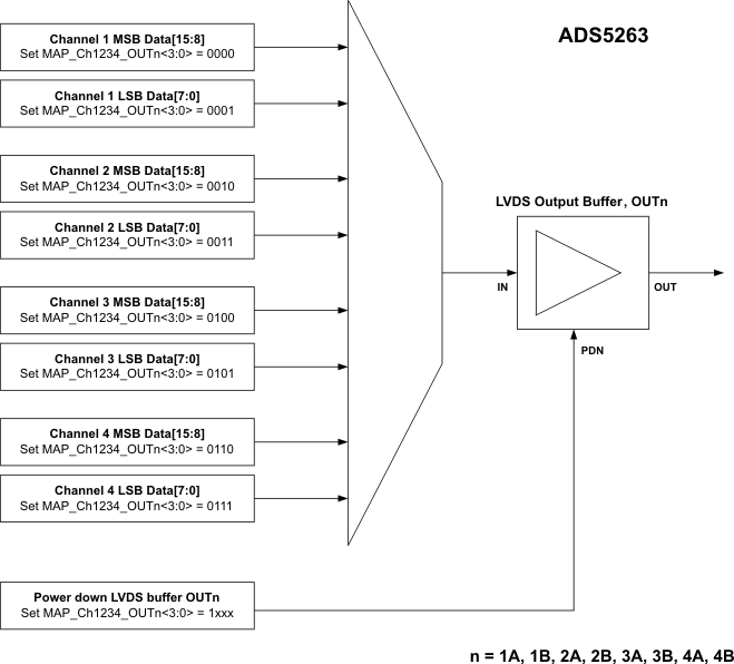 Figure 51. Mapping in 2-Wire Interface
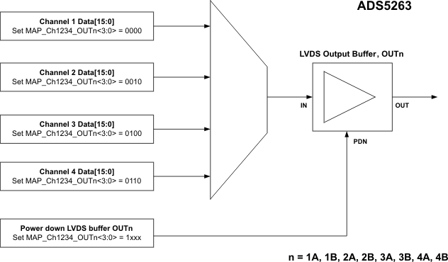 Figure 52. Mapping in 1-Wire Interface
8.3.8 Output LVDS Interface
The ADS5263 offers several flexible output options, making it easy to interface to an ASIC or an FPGA. Each of these options can be easily programmed using the serial interface. A summary of all the options is presented in Table 7, along with the default values after power up and reset. Following this, each option is described in detail.
The output interface options are:
- 1-wire, 16× serialization with DDR bit clock and 1× frame clock
- The 16-bit ADC data is serialized and output over one LVDS pair per channel together with an 8× bit clock and 1× frame clock. The output data rate is 16× sample rate; hence, it is suited for low sample rates, typically up to 50 MSPS.
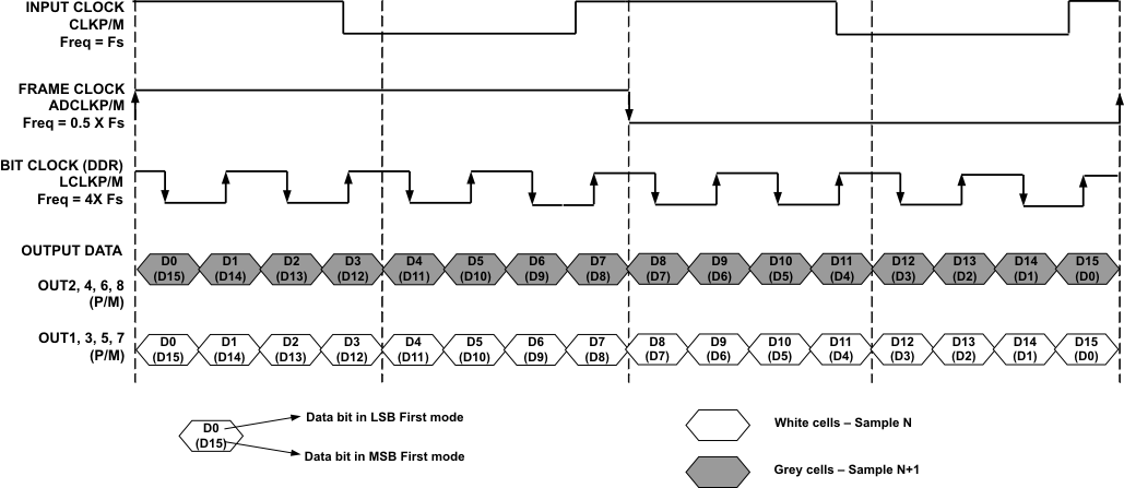
- 2-wire, 8× serialization with DDR bit clock and 0.5× frame clock (16 bit ADC mode, Figure 54 and Figure 55)
- Here, the 16 bit ADC data is serialized and output over two LVDS pairs per channel. The output data rate is 8x sample rate, with a 4x bit clock and 0.5x frame clock.
Because the output data rate is half compared to the 1-wire case, this interface can be used up to the maximum sample rate of the device.
- Here, the 16 bit ADC data is serialized and output over two LVDS pairs per channel. The output data rate is 8x sample rate, with a 4x bit clock and 0.5x frame clock.
- 2-wire, 8× serialization with DDR bit clock and 0.5× frame clock (14-bit ADC mode)
- Here, the 14-bit ADC data is padded with two zero bits. The combined 16-bit data is then serialized and output over two LVDS pairs per channel. The output data rate is 8× sample rate, with a 4× bit clock and 0.5× frame clock Because the output data rate is half compared to the 1-wire case, this interface can be used up to the maximum sample rate of the device.
- 1-wire, 14× serialization with DDR bit clock and 1× frame clock (14-bit ADC mode)
- The 14-bit ADC data is serialized and output over one LVDS pair per channel together with a 7× bit clock and 1× frame clock. The output data rate is 14× sample rate; hence, it is suited for low sample rates, typically up to 50 MSPS.
- 2-wire, 7× serialization with DDR bit clock and 0.5× frame clock (14-bit ADC mode, Figure 57 and Figure 58)
- Here, the 14-bit ADC data is serialized and output over two LVDS pairs per channel. The output data rate is 7× sample rate, with a 3.5× bit clock and 0.5× frame clock. Because the output data rate is half compared to the 1-wire case, this interface can be used up to the maximum sample rate of the device.
- 1-wire, 18× serialization with DDR bit clock and 1× frame clock – Here, the 18-bit data from the digital processing block is serialized and output over one LVDS pair per channel, together with a 9× bit clock and 1x frame clock. The output data rate is 18× sample rate; hence, it is suited for low sample rates, typically up to 40 MSPS. This interface is primarily intended to be used when the averaging and digital filters are enabled.
Table 7. Summary of Output Interface Options
| FEATURE | OPTIONS | AVAILABLE IN | DEFAULT AFTER POWER UP AND RESET | BRIEF DESCRIPTION | |
|---|---|---|---|---|---|
| 1 wire | 2 wire | ||||
| Wire interface | 1 wire and 2 wire |
1 wire | 1 wire – ADC data is sent serially over one pair of LVDS pins 2 wire – ADC data is split and sent serially over two pairs of LVDS pins |
||
| Serialization factor | 16× | X | X | 16× | For 16-bit ADC mode Can also be used with 14-bit ADC mode – the 14-bit ADC data is padded with two zeros and the combined 16-bit data is serialized. |
| 18× | X | 18-bit data is available when 16-bit ADC mode is used with averaging and decimation filters enabled. | |||
| 14× | X | X | For 14-bit ADC mode only | ||
| DDR bit-clock frequency | 8× | X | 8× | 16× serialization | |
| 4× | X | 16× serialization Only with 2-wire interface |
|||
| 9× | X | 18× serialization | |||
| 7× | X | 14× serialization | |||
| 3.5× | X | 14× serialization Only with 2-wire interface |
|||
| Frame-clock frequency | 1× sample rate | X | 1× | ||
| 1/2× sample rate | X | ||||
| Bit sequence | Bytewise | X | — | Bytewise – The ADC data is split into upper and lower bytes, which are output on separate wires. Bitwise – The ADC data is split into even and odd bits, which are output on separate wires. Wordwise – Successive ADC data samples are sent over separate wires. These options are available only with 2-wire interface. |
|
| Bitwise | X | ||||
| Wordwise | X | ||||
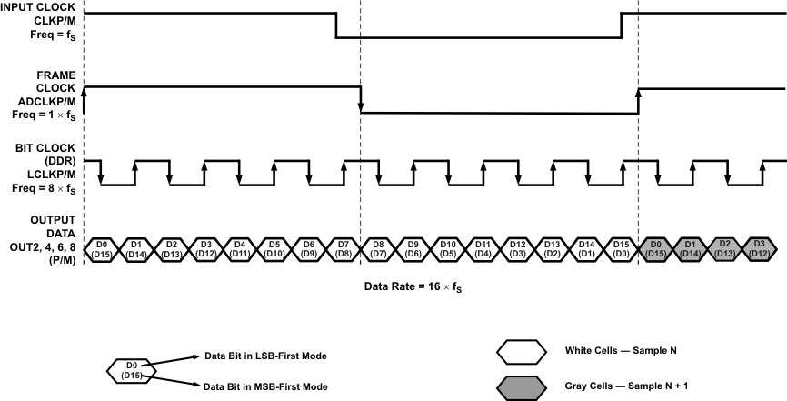 Figure 53. Output LVDS Interface, 1-Wire, 16× Serialization
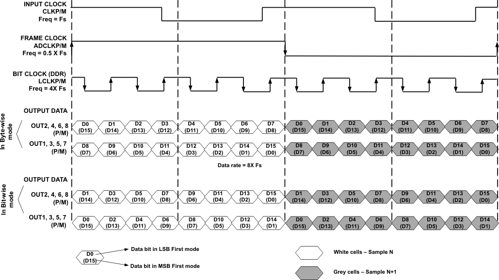 Figure 54. LVDS Output Interface, 2-Wire, 8× Serialization, Bytewise and Bitwise Modes
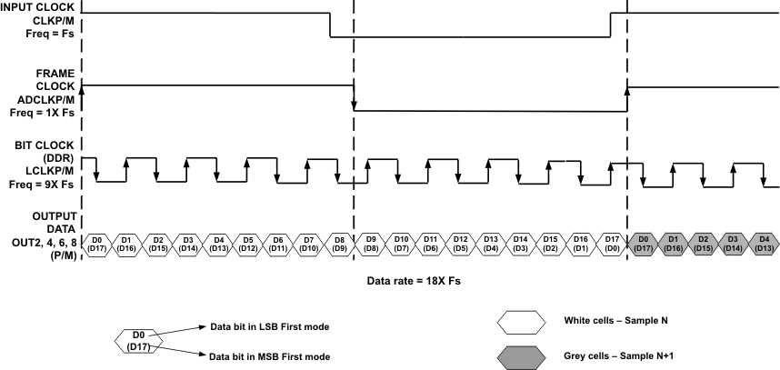 Figure 56. LVDS Output Interface, 1-Wire, 18× Serialization
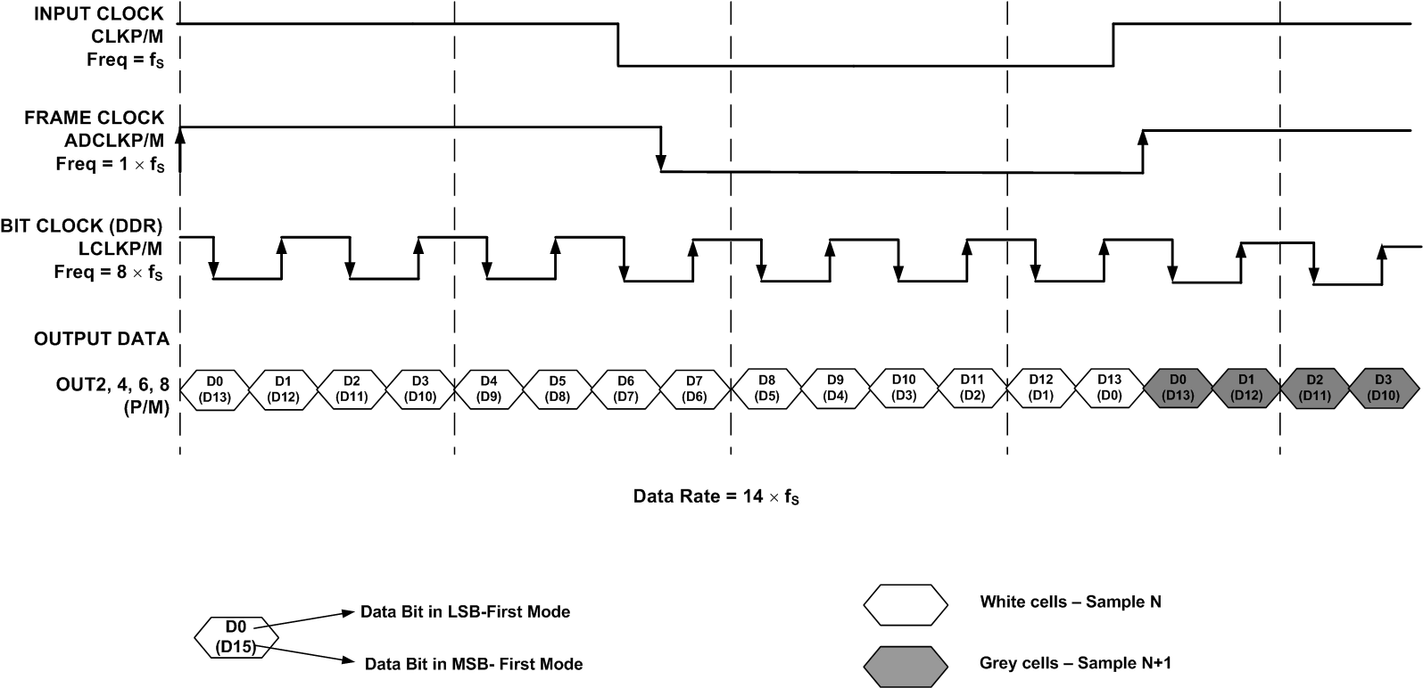 Figure 57. LVDS Output Interface, 1-Wire, 14× Serialization
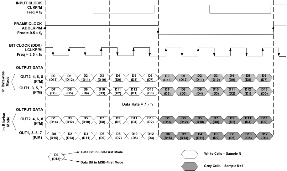 Figure 58. LVDS Output Interface, 2-Wire, 7× Serialization
8.3.9 Programmable LCLK Phase
The ADS5263 allows programmability of the edge of the output bit clock (LCLK) using register bits <PHASE_DDR> as follows:
The default value of PHASE_DDR after reset is 10, and the default phase corresponds to Figure 59.
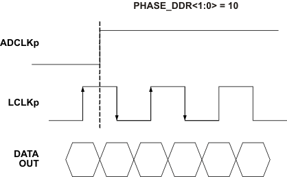 Figure 59. Default LCLK Phase
The phase can also be changed to one of the following states by changing the value of the <PHASE_DDR1:0> bits (and setting register bit EN_REG_42 = 1).
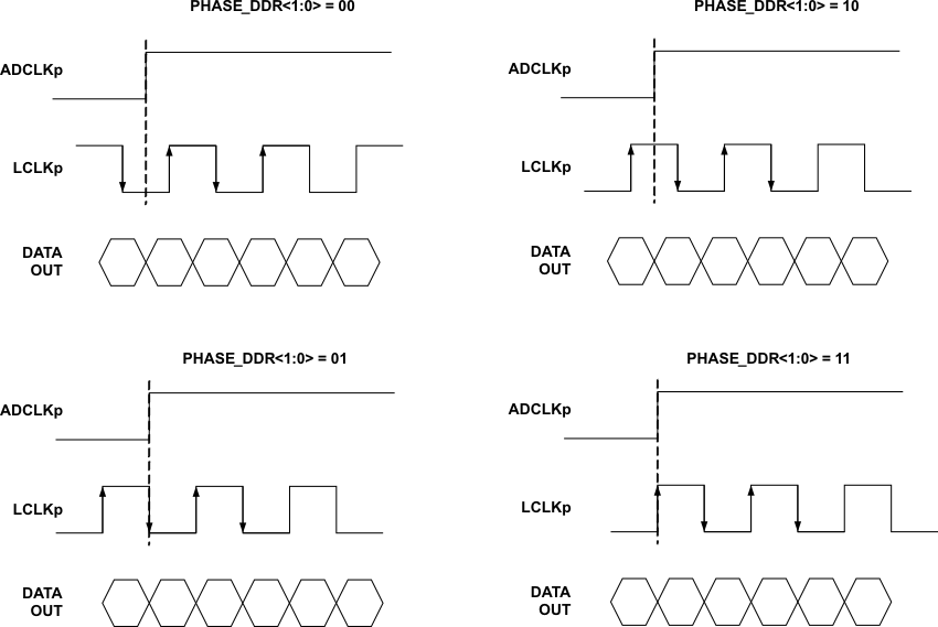 Figure 60. Programmable LCLK Phases
8.4 Device Functional Modes
8.4.1 Device Configuration
ADS5263 has several modes that can be configured using a serial programming interface, as described below. In addition, the device has dedicated parallel pins for controlling common functions such as power down and internal or external reference selection.
Table 8. PDN CONTROL PIN
| VOLTAGE APPLIED ON PDN | STATE OF REGISTER BIT <CONFIG PDN pin> |
DESCRIPTION |
|---|---|---|
| 0 V | X (don't care) | Normal operation |
| Logic HIGH | 0 | Device enters global power-down mode |
| 1 | Device enters standby mode |
Table 9. INT/EXT CONTROL PIN
| VOLTAGE APPLIED ON INT/EXT | DESCRIPTION |
|---|---|
| 0 V | External reference mode. Apply voltage on VCM pin to set the references for ADC operation. |
| Logic HIGH | Internal reference |
8.4.2 Serial Register Readout
The device includes a mode where the contents of the internal registers can be read back on SDOUT pin. This may be useful as a diagnostic check to verify the serial interface communication between the external controller and the ADC.
By default, after power up and device reset, the SDOUT pin is in the high-impedance state. When the readout mode is enabled using the register bit <READOUT>, SDOUT outputs the contents of the selected register serially, described as follows.
- Set register bit <READOUT> = 1 to put the device in serial readout mode. This disables any further writes into the internal registers, EXCEPT the register at address 1. Note that the <READOUT> bit itself is also located in register 1.
The device can exit readout mode by writing <READOUT> to 0.
Only the contents of register at address 1 cannot be read in the register readout mode. - Initiate a serial interface cycle specifying the address of the register (A7-A0) whose content is to be read.
- The device serially outputs the contents (D15–D0) of the selected register on the SDOUT pin.
- The external controller can latch the contents at the rising edge of SCLK.
- To exit the serial readout mode, reset register bit <READOUT> = 0, which enables writes into all registers of the device. At this point, the SDOUT pin enters the high-impedance state.
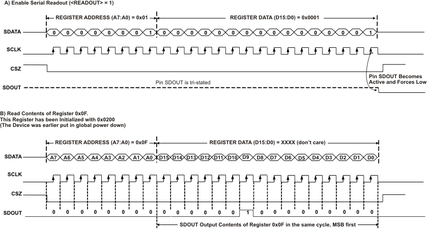 Figure 61. Serial Readout Timing
8.5 Programming
8.5.1 Serial Interface
The ADC has a set of internal registers, which can be accessed by the serial interface formed by pins CS (serial interface enable), SCLK (serial interface clock) and SDATA (serial interface data).
When CS is low,
- Serial shift of bits into the device is enabled.
- Serial data (on SDATA pin) is latched at every rising edge of SCLK.
- The serial data is loaded into the register at every 24th SCLK rising edge.
In case the word length exceeds a multiple of 24 bits, the excess bits are ignored. Data can be loaded in multiples of 24-bit words within a single active CS pulse.
The first 8 bits form the register address and the remaining 16 bits form the register data. The interface can work with SCLK frequencies from 20 MHz down to very low speeds (a few hertz) and also with non-50% SCLK duty cycle.
8.5.2 Register Initialization
After power up, the internal registers MUST be initialized to their default values. This can be done in one of two ways:
- Through a hardware reset by applying a low-going pulse on the RESET pin (of width greater than 10 ns) as shown in Figure 62.
- By applying software reset. Using the serial interface, set the <RESET> bit (D7 in register 0x00) to HIGH. This initializes internal registers to their default values and then self-resets the <RESET> bit to low. In this case, the RESET pin is kept high (inactive).
OR
 Figure 62. Serial Interface Timing
8.6 Register Maps
Table 10. Summary of Functions Supported by Serial Interface(1)
| Register Address | Register Data(2) | |||||||||||||||
|---|---|---|---|---|---|---|---|---|---|---|---|---|---|---|---|---|
| A7-A0 in HEX | D15 | D14 | D13 | D12 | D11 | D10 | D9 | D8 | D7 | D6 | D5 | D4 | D3 | D2 | D1 | D0 |
| 0 | 0 | 0 | 0 | 0 | 0 | 0 | 0 | 0 | 0 | 0 | 0 | 0 | 0 | 0 | 0 | <RESET> |
| 1 | 0 | 0 | 0 | 0 | 0 | 0 | 0 | 0 | 0 | 0 | 0 | <EN
_HIGH _ADDRS> |
0 | 0 | 0 | <READOUT> |
| 2 | 0 | 0 | <EN SYNC> | 0 | 0 | 0 | 0 | 0 | 0 | 0 | 0 | 0 | 0 | 0 | 0 | 0 |
| 9 | 0 | 0 | 0 | 0 | 0 | <EN
_CLAMP> |
0 | 0 | 0 | 0 | 0 | 0 | 0 | 0 | 0 | 0 |
| F | 0 | 0 | 0 | 0 | 0 | <CONFIG PD PIN> | <GLOBAL PDN> | <STANDBY> | <PDN
CH 4B> |
<PDN
CH 3B> |
<PDN
CH 2B> |
<PDN
CH 1B> |
<PDN
CH 4A> |
<PDN
CH 3A> |
<PDN
CH 2A> |
<PDN
CH 1A> |
| 11 | 0 | 0 | 0 | 0 | 0 | <LVDS CURR DATA> | 0 | <LVDS CURR ADCLK> | 0 | <LVDS CURR LCLK> | ||||||
| 12 | 0 | <ENABLE LVDS TERM> | 0 | 0 | 0 | <LVDS TERM DATA> | 0 | <LVDS TERM ADCLK> | 0 | <LVDS TERM LCLK> | ||||||
| 14 | 0 | 0 | 0 | 0 | 0 | 0 | 0 | 0 | 0 | 0 | 0 | 0 | <EN LFNS CH 4> | <EN LFNS CH 3> | <EN LFNS CH 2> | <EN LFNS
CH 1> |
| 25 | 0 | 0 | 0 | 0 | 0 | 0 | 0 | 0 | 0 | <RAMP TEST PATTERN> | <DUAL CUSTOM PATTERN> | <SINGLE CUSTOM PATTERN> | CUSTOM PATTERN B DATA[15...14] | CUSTOM PATTERN A DATA[15...14] | ||
| 26 | CUSTOM PATTERN A DATA[13..0] | 0 | 0 | |||||||||||||
| 27 | CUSTOM PATTERN B DATA[13..0] | 0 | 0 | |||||||||||||
| 28 | <EN WORD- WISE CONTROL> | <WORD-WISE CH4 | <WORD-WISE CH3> | <WORD-WISE CH2> | <WORD-WISE CH1> | |||||||||||
| 29 | 0 | 0 | 0 | 0 | 0 | 0 | 0 | 0 | 0 | 0 | 0 | 0 | 0 | 0 | <EN DIG FILTER> | <EN AVG> |
| 2A | <GAIN CH4> | <GAIN CH3> | <GAIN CH2> | <GAIN CH1> | ||||||||||||
| 2C | 0 | 0 | 0 | 0 | 0 | 0 | 0 | 0 | <AVG OUT 4> | <AVG OUT 3> | <AVG OUT 2> | <AVG OUT 1> | ||||
| 2E | 0 | 0 | 0 | 0 | 0 | 0 | <FILTER TYPE CH1> | <DEC by RATE CH1> | 0 | <ODD TAP CH1> | 0 | <USE FILTER CH1> | ||||
| 2F | 0 | 0 | 0 | 0 | 0 | 0 | <FILTER TYPE CH2> | <DEC by RATE CH2> | 0 | <ODD TAP CH2> | 0 | <USE FILTER CH2> | ||||
| 30 | 0 | 0 | 0 | 0 | 0 | 0 | <FILTER TYPE CH3> | <DEC by RATE CH3> | 0 | <ODD TAP CH3> | 0 | <USE FILTER CH3> | ||||
| 31 | 0 | 0 | 0 | 0 | 0 | 0 | <FILTER TYPE CH4> | <DEC by RATE CH4> | 0 | <ODD TAP CH4> | 0 | <USE FILTER CH4> | ||||
| 38 | 0 | 0 | 0 | 0 | 0 | 0 | 0 | 0 | 0 | 0 | 0 | 0 | 0 | 0 | <OUTPUT RATE> | |
| 42 | <EN_REG_42> | 0 | 0 | 0 | 0 | 0 | 0 | 0 | 0 | <PHASE_DDR> | 0 | <EXT_REF_VCM> | 0 | 0 | 0 | |
| 45 | 0 | 0 | 0 | 0 | 0 | 0 | 0 | 0 | 0 | 0 | 0 | 0 | 0 | 0 | <SYNC PATTERN> | <DESKEW PATTERN> |
| 46 | <EN SERIALI
ZATION> |
0 | 0 | <18x SERIALI
ZATION> |
<16× SERIALI
ZATION> |
<14× SERIALI
ZATION> |
0 | 0 | 0 | 0 | <PAD two 0s> | 0 | <MSB FIRST> | <2S COMPL> | 0 | <2-WIRE 0.5X FRAME> |
| 50 | <EN MAP1> | 0 | 0 | 0 | <MAP_Ch1234_OUT2A> | <MAP_Ch1234_OUT1B> | <MAP_Ch1234_OUT1A> | |||||||||
| 51 | <EN MAP2> | 0 | 0 | 0 | <MAP_Ch1234_OUT3B> | <MAP_Ch1234_OUT3A> | <MAP_Ch1234_OUT2B> | |||||||||
| 52 | <EN MAP3> | 0 | 0 | 0 | 0 | 0 | 0 | 0 | <MAP_Ch1234_OUT4B> | <MAP_Ch1234_OUT4A> | ||||||
| 57 | 0 | 0 | 0 | 0 | 0 | 0 | 0 | 0 | 0 | 0 | <DIS STATIC OFFSET CORR> | 0 | 0 | 0 | 0 | 0 |
| 5A to 65 | <EN CUSTOM FILT CH1> | <COEFFn SET CH1>(3) | ||||||||||||||
| 66 to 71 | <EN CUSTOM FILT CH2> | <COEFFn SET CH2>(3) | ||||||||||||||
| 72 to 7D | <EN CUSTOM FILT CH3> | <COEFFn SET CH3>(3) | ||||||||||||||
| 7E to 89 | <EN CUSTOM FILT CH4> | <COEFFn SET CH4>(3) | ||||||||||||||
| CB | <EN DITH1> | 0 | 0 | 0 | 0 | 0 | 0 | <EN DITH2> | <EN DITH3> | 0 | 0 | 0 | 0 | 0 | 0 | 0 |
| B3 | <EN ADC MODE> | 0 | 0 | 0 | 0 | 0 | 0 | 0 | 0 | 0 | 0 | 0 | 0 | 0 | 0 | <16B/14B ADC MODE> |
| F0 | <EN_EXT_REF> | 0 | 0 | 0 | 0 | 0 | 0 | 0 | 0 | 0 | 0 | 0 | 0 | 0 | 0 | 0 |
8.6.1 Default State After Reset
- Device is in normal operation mode with 16-bit ADC enabled for all 4 channels.
- Output interface is 1-wire, 16× serialization with 8× bit clock and 1× frame clock frequency
- Serial readout is disabled
- PD pin is configured as global power-down pin
- LVDS output current is set to 3.5 mA; internal termination is disabled.
- Digital gain is set to 0 dB.
- Digital modes such as LFNS, digital filters are disabled.
8.6.2 Description of Serial Registers
| REGISTER ADDRESS | REGISTER DATA | |||||||||||||||
|---|---|---|---|---|---|---|---|---|---|---|---|---|---|---|---|---|
| A7–A0 IN HEX |
D15 | D14 | D13 | D12 | D11 | D10 | D9 | D8 | D7 | D6 | D5 | D4 | D3 | D2 | D1 | D0 |
| 0 | 0 | 0 | 0 | 0 | 0 | 0 | 0 | 0 | 0 | 0 | 0 | 0 | 0 | 0 | 0 | <RESET> |
| D0 | <RESET> |
| 1 | Software reset applied – resets all internal registers to their default values and self-clears to 0 |
| A7–A0 IN HEX |
D15 | D14 | D13 | D12 | D11 | D10 | D9 | D8 | D7 | D6 | D5 | D4 | D3 | D2 | D1 | D0 |
|---|---|---|---|---|---|---|---|---|---|---|---|---|---|---|---|---|
| 1 | 0 | 0 | 0 | 0 | 0 | 0 | 0 | 0 | 0 | 0 | 0 | <EN
_HIGH _ADDRS> |
0 | 0 | 0 | <READOUT> |
| D4 | <EN_HIGH_ADDRS> |
| See section External Reference Mode | |
| D0 | <READOUT> |
| 0 | Serial readout of registers is disabled. Pin SDOUT is in the high-impedance state. |
| 1 | Serial readout enabled, SDOUT pin functions as serial data readout. |
| A7–A0 IN HEX |
D15 | D14 | D13 | D12 | D11 | D10 | D9 | D8 | D7 | D6 | D5 | D4 | D3 | D2 | D1 | D0 |
|---|---|---|---|---|---|---|---|---|---|---|---|---|---|---|---|---|
| 2 | 0 | 0 | <EN SYNC> | 0 | 0 | 0 | 0 | 0 | 0 | 0 | 0 | 0 | 0 | 0 | 0 | 0 |
| D13 | <EN SYNC> |
| 0 | SYNC pin is disabled. |
| 1 | SYNC pin can be used to synchronize the decimation filters across channels and across multiple chips. |
| A7–A0 IN HEX |
D15 | D14 | D13 | D12 | D11 | D10 | D9 | D8 | D7 | D6 | D5 | D4 | D3 | D2 | D1 | D0 |
|---|---|---|---|---|---|---|---|---|---|---|---|---|---|---|---|---|
| 9 | 0 | 0 | 0 | 0 | 0 | <EN
_CLAMP> |
0 | 0 | 0 | 0 | 0 | 0 | 0 | 0 | 0 | 0 |
| A7–A0 IN HEX |
D15 | D14 | D13 | D12 | D11 | D10 | D9 | D8 | D7 | D6 | D5 | D4 | D3 | D2 | D1 | D0 |
|---|---|---|---|---|---|---|---|---|---|---|---|---|---|---|---|---|
| F | 0 | 0 | 0 | 0 | 0 | <CONFIG
PD PIN> |
<GLOBAL
PDN> |
<STAND
BY> |
<PDN
CH 4B> |
<PDN
CH 3B> |
<PDN
CH 2B> |
<PDN
CH 1B> |
<PDN
CH 4A> |
<PDN
CH 3A> |
<PDN
CH 2A> |
<PDN
CH 1A> |
| D10 | <CONFIG PDN PIN> Can be used to configure PDN pin as global power down or standby |
| 0 | PDN pin functions as global power down. |
| 1 | PDN pin functions as standby. |
| D9 | <GLOBAL PDN> |
| 0 | Normal ADC operation |
| 1 | Device is put in global power down. All four channels are powered down, including LVDS output data and clock buffers. |
| D8 | <STANDBY> |
| 0 | Normal ADC operation |
| 1 | Device is put in standby. All four ADCs are powered down. Internal PLL, LVDS bit clock, and frame clock are running. |
| D7–D0 | <PDN CH X> Individual channel power down |
| 0 | Channel X is powered up. |
| 1 | Channel X is powered down. |
| REGISTER ADDRESS | REGISTER DATA | |||||||||||||||
|---|---|---|---|---|---|---|---|---|---|---|---|---|---|---|---|---|
| A7–A0 IN HEX |
D15 | D14 | D13 | D12 | D11 | D10 | D9 | D8 | D7 | D6 | D5 | D4 | D3 | D2 | D1 | D0 |
| 11 | 0 | 0 | 0 | 0 | 0 | <LVDS CURR DATA> | 0 | <LVDS CURR ADCLK> | 0 | <LVDS CURR LCLK> | ||||||
| D10–D8 | <LVDS CURR DATA> LVDS current control for data buffers |
| 000 | 3.5 mA |
| 001 | 2.5 mA |
| 010 | 1.5 mA |
| 011 | 0.5 mA |
| 100 | 7.5 mA |
| 101 | 6.5 mA |
| 110 | 5.5 mA |
| 111 | 4.5 mA |
| D6–D4 | <LVDS CURR LCLK> LVDS current control for frame-clock buffer |
| 000 | 3.5 mA |
| 001 | 2.5 mA |
| 010 | 1.5 mA |
| 011 | 0.5 mA |
| 100 | 7.5 mA |
| 101 | 6.5 mA |
| 110 | 5.5 mA |
| 111 | 4.5 mA |
| D2–D0 | <LVDS CURR LCLK> LVDS current control for bit-clock buffer |
| 000 | 3.5 mA |
| 001 | 2.5 mA |
| 010 | 1.5 mA |
| 011 | 0.5 mA |
| 100 | 7.5 mA |
| 101 | 6.5 mA |
| 110 | 5.5 mA |
| 111 | 4.5 mA |
| REGISTER ADDRESS | REGISTER DATA | |||||||||||||||
|---|---|---|---|---|---|---|---|---|---|---|---|---|---|---|---|---|
| A7–A0 IN HEX |
D15 | D14 | D13 | D12 | D11 | D10 | D9 | D8 | D7 | D6 | D5 | D4 | D3 | D2 | D1 | D0 |
| 12 | 0 | <ENABLE LVDS TERM> | 0 | 0 | 0 | <LVDS TERM DATA> | 0 | <LVDS TERM ADCLK> | 0 | <LVDS TERM LCLK> | ||||||
| D14 | <ENABLE LVDS TERM> |
| 0 | Internal termination disabled |
| 1 | Internal termination enabled |
| D10–D8 | <LVDS TERM DATA> Internal LVDS termination for data buffers |
| 000 | No internal termination |
| 001 | 150 Ω |
| 010 | 100 Ω |
| 011 | 60 Ω |
| 100 | 80 Ω |
| 101 | 55 Ω |
| 110 | 45 Ω |
| 111 | 35 Ω |
| D6–D4 | <LVDS TERM ADCLK> Internal LVDS termination for frame clock buffer |
| 000 | No internal termination |
| 001 | 150 Ω |
| 010 | 100 Ω |
| 011 | 60 Ω |
| 100 | 80 Ω |
| 101 | 55 Ω |
| 110 | 45 Ω |
| 111 | 35 Ω |
| D2–D0 | <LVDS TERM LCLK> Internal LVDS termination for bit clock buffer |
| 000 | No internal termination |
| 001 | 150 Ω |
| 010 | 100 Ω |
| 011 | 60 Ω |
| 100 | 80 Ω |
| 101 | 55 Ω |
| 110 | 45 Ω |
| 111 | 35 Ω |
| REGISTER ADDRESS | REGISTER DATA | |||||||||||||||
|---|---|---|---|---|---|---|---|---|---|---|---|---|---|---|---|---|
| A7–A0 IN HEX |
D15 | D14 | D13 | D12 | D11 | D10 | D9 | D8 | D7 | D6 | D5 | D4 | D3 | D2 | D1 | D0 |
| 14 | 0 | 0 | 0 | 0 | 0 | 0 | 0 | 0 | 0 | 0 | 0 | 0 | <EN LFNS CH4> | <EN LFNS CH3> | <EN LFNS CH2> | <EN LFNS CH1> |
| D3–D0 | <EN LFNS CH X> low-frequency noise-suppression mode is enabled for channel X. |
| 0 | LFNS mode is disabled. |
| 1 | LFNS mode is enabled for channel X. |
| In 16-bit ADC mode, <EN LFNS CH X> enables LFNS for channel CH X. | |
| In 14-bit ADC mode, <EN LFNS CH X> enables LFNS for channel CH X B. | |
| A7–A0 IN HEX |
D15 | D14 | D13 | D12 | D11 | D10 | D9 | D8 | D7 | D6 | D5 | D4 | D3 | D2 | D1 | D0 |
|---|---|---|---|---|---|---|---|---|---|---|---|---|---|---|---|---|
| 25 | 0 | 0 | 0 | 0 | 0 | 0 | 0 | 0 | 0 | <RAMP TEST PATTERN> | <DUAL CUSTOM PATTERN> | <SINGLE CUSTOM PATTERN> | CUSTOM PATTERN B
DATA[15...14] |
CUSTOM PATTERN A
DATA[15...14] |
||
| D6 | <RAMP TEST PATTERN> |
| 0 | Ramp test pattern is disabled. |
| 1 | Ramp test pattern is enabled; output code increments by one LSB every clock cycle. |
| D5 | <DUAL CUSTOM PATTERN> |
| 0 | Dual custom pattern is disabled. |
| 1 | Dual custom pattern is enabled. |
| Two custom patterns can be specified in registers PATTERN A and PATTERN B. The two patterns are output one after the other (instead of ADC data). | |
| D5 | <SINGLE CUSTOM PATTERN> |
| 0 | Single custom pattern is disabled. |
| 1 | Single custom pattern is enabled. |
| The custom pattern can be specified in register A and is output every clock cycle instead of ADC data. | |
| D3–D2 | <CUSTOM PATTERN B bits D15 and D14> |
| D1–D0 | <CUSTOM PATTERN A bits D15 and D14> |
| Specify bits D15 and D14 of custom pattern in these register bits. |
| A7–A0 IN HEX |
D15 | D14 | D13 | D12 | D11 | D10 | D9 | D8 | D7 | D6 | D5 | D4 | D3 | D2 | D1 | D0 |
|---|---|---|---|---|---|---|---|---|---|---|---|---|---|---|---|---|
| 26 | CUSTOM PATTERN A DATA[13..0] | 0 | 0 | |||||||||||||
| 27 | CUSTOM PATTERN B DATA[13..0] | 0 | 0 | |||||||||||||
| Specify bits D13 to D0 of custom pattern in these registers. |
| A7–A0 IN HEX |
D15 | D14 | D13 | D12 | D11 | D10 | D9 | D8 | D7 | D6 | D5 | D4 | D3 | D2 | D1 | D0 |
|---|---|---|---|---|---|---|---|---|---|---|---|---|---|---|---|---|
| 28 | <EN WORD-WISE CONTROL> | <WORD-WISE CH4> | <WORD-WISE CH3> | <WORD-WISE CH2> | <WORD-WISE CH1> |
| D15 | <EN WORD-WISE CONTROL> |
| 0 | Control of word-wise mode is disabled. |
| 1 | Control of word-wise mode is enabled. |
| D3–D0 | <WORD-WISE CH XL> |
| 0 | Output data is serially sent in byte-wise format. |
| 1 | Output data is serially sent in word-wise format ONLY when 2-wire mode is enabled (see register 0x46). |
| A7–A0 IN HEX |
D15 | D14 | D13 | D12 | D11 | D10 | D9 | D8 | D7 | D6 | D5 | D4 | D3 | D2 | D1 | D0 |
|---|---|---|---|---|---|---|---|---|---|---|---|---|---|---|---|---|
| 2A | <GAIN CH4> | <GAIN CH3> | <GAIN CH2> | <GAIN CH1> | ||||||||||||
| <GAIN CH x> Individual channel gain control | |
| In 16-bit ADC mode, <GAIN CH X> sets gain for channel CH X A. | |
| In 14-bit ADC mode, <GAIN CH X> sets gain for channel CH X B. | |
| 0000 | 0 dB |
| 0001 | 1 dB |
| 0010 | 2 dB |
| 0011 | 3 dB |
| 0100 | 4 dB |
| 0101 | 5 dB |
| 0110 | 6 dB |
| 0111 | 7 dB |
| 1000 | 8 dB |
| 1001 | 9 dB |
| 1010 | 10 dB |
| 1011 | 11 dB |
| 1100 | 12 dB |
| 1101 to 1111 | Unused |
| A7–A0 IN HEX |
D15 | D14 | D13 | D12 | D11 | D10 | D9 | D8 | D7 | D6 | D5 | D4 | D3 | D2 | D1 | D0 |
|---|---|---|---|---|---|---|---|---|---|---|---|---|---|---|---|---|
| 2C | 0 | 0 | 0 | 0 | 0 | 0 | 0 | 0 | <AVG OUT 4> | <AVG OUT 3> | <AVG OUT 2> | <AVG OUT 1> | ||||
| <AVG OUT 1> | These bits determine which data stream is output on LVDS pins OUT1A/1B. |
| (after global enable bit for averaging is enabled <EN AVG GLO> = 1) | |
| 00 | LVDS OUT1A/1B buffers are powered down. |
| 01 | OUT1A/1B output digital data corresponding to the signal applied on analog input pin IN1. |
| 10 | OUT1A/1B output digital data corresponding to the average of signals applied on analog input pins IN1 and IN2. |
| 11 | OUT1A/1B output digital data corresponding to the average of signals applied on analog input pins IN1, IN2, IN3, and IN4. |
| <AVG OUT 2> | These bits determine which data stream is output on LVDS pins OUT2A/2B |
| (after global enable bit for averaging is enabled <EN AVG GLO> = 1) | |
| 00 | LVDS OUT2A/2B buffers are powered down. |
| 01 | OUT2A/2B output digital data corresponding to the signal applied on analog input pin IN2. |
| 10 | OUT2A/2B output digital data corresponding to the signal applied on analog input pin IN3. |
| 11 | OUT2A/2B output digital data corresponding to the average of signals applied on analog input pins IN3 and IN4. |
| <AVG OUT 3> | These bits determine which data stream is output on LVDS pins OUT3A/3B |
| (after global enable bit for averaging is enabled <EN AVG GLO> = 1) | |
| 00 | LVDS OUT3A/3B buffers are powered down. |
| 01 | OUT3A/3B output digital data corresponding to the signal applied on analog input pin IN3. |
| 10 | OUT3A/3B output digital data corresponding to the signal applied on analog input pin IN2. |
| 11 | OUT3A/3B output digital data corresponding to the average of signals applied on analog input pins IN1 and IN4. |
| <AVG OUT 4> | These bits determine which data stream is output on LVDS pins OUT4A/4B |
| (after global enable bit for averaging is enabled <EN AVG GLO> = 1) | |
| 00 | LVDS OUT4A/4B buffers are powered down. |
| 01 | OUT4A/4B output digital data corresponding to the signal applied on analog input pin IN4. |
| 10 | OUT4A/4B output digital data corresponding to the average of signals applied on analog input pins IN3 and IN4. |
| 11 | OUT4A/4B output digital data corresponding to the average of signals applied on analog input pins IN1, IN2, IN3, and IN4. |
| A7–A0 IN HEX |
D15 | D14 | D13 | D12 | D11 | D10 | D9 | D8 | D7 | D6 | D5 | D4 | D3 | D2 | D1 | D0 |
|---|---|---|---|---|---|---|---|---|---|---|---|---|---|---|---|---|
| 29 | 0 | 0 | 0 | 0 | 0 | 0 | 0 | 0 | 0 | 0 | 0 | 0 | 0 | 0 | <EN DIG FILTER> | <EN AVG GLO> |
| D1 | <EN DIG FILTER> |
| 0 | Digital filter mode is disabled. |
| 1 | Digital filter mode is enabled on all channels. To turn filter on or off for individual channels, also set the <USE FILTER CH X> register bit. |
| D0 | <EN AVG GLO> |
| 0 | Averaging mode is disabled. |
| 1 | Averaging mode is enabled on all channels. |
| A7–A0 IN HEX |
D15 | D14 | D13 | D12 | D11 | D10 | D9 | D8 | D7 | D6 | D5 | D4 | D3 | D2 | D1 | D0 |
|---|---|---|---|---|---|---|---|---|---|---|---|---|---|---|---|---|
| 2E | 0 | 0 | 0 | 0 | 0 | 0 | <FILTER TYPE CH1> | <DEC by RATE CH1> | 0 | 0 | 0 | <USE FILTER CH1> | ||||
| 2F | 0 | 0 | 0 | 0 | 0 | 0 | <FILTER TYPE CH2> | <DEC by RATE CH2> | 0 | 0 | 0 | <USE FILTER CH2> | ||||
| 30 | 0 | 0 | 0 | 0 | 0 | 0 | <FILTER TYPE CH3> | <DEC by RATE CH3> | 0 | 0 | 0 | <USE FILTER CH3> | ||||
| 31 | 0 | 0 | 0 | 0 | 0 | 0 | <FILTER TYPE CH4> | <DEC by RATE CH4> | 0 | 0 | 0 | <USE FILTER CH4> | ||||
| D0 | <USE FILTER CH X> |
| 0 | Filter is turned OFF on channel X |
| 1 | Filter is turned ON on channel X. |
| D2 | <ODD TAP CH X> select filter with even or odd tap for channel X |
| 0 | Even tap filter is selected. |
| 1 | Odd tap filter is selected. |
| D6–D4 | <DEC by RATE CH X> select decimation rates for channel X |
| 000 | Decimate-by-2 rate is selected. |
| 001 | Decimate-by-4 rate is selected. |
| 100 | Decimate-by-8 rate is selected. |
| Other combinations x Do not use | |
| D9–D7 | <FILTER TYPE CH X> select type of filter for channel X |
| 000 | Low-pass filter with decimate-by-2 rate |
| 001 | High-pass filter with decimate-by-2 rate |
| 010 | Low-pass filter with decimate-by-4 rate |
| 011 | Band-pass filter #1 with decimate-by-4 rate |
| 100 | Band-pass filter #2 with decimate-by-4 rate |
| 101 | High-pass filter with decimate-by-4 rate |
| A7–A0 IN HEX |
D15 | D14 | D13 | D12 | D11 | D10 | D9 | D8 | D7 | D6 | D5 | D4 | D3 | D2 | D1 | D0 |
|---|---|---|---|---|---|---|---|---|---|---|---|---|---|---|---|---|
| 38 | 0 | 0 | 0 | 0 | 0 | 0 | 0 | 0 | 0 | 0 | 0 | 0 | 0 | 0 | <OUTPUT RATE> | |
| D1–D0 | <OUTPUT RATE> |
| 00 | Output data rate = 1× sample rate |
| 01 | Output data rate = 0.5× sample rate |
| 02 | Output data rate = 0.25× sample rate |
| 03 | Output data rate = 0.125× sample rate |
| REGISTER ADDRESS | REGISTER DATA | |||||||||||||||
|---|---|---|---|---|---|---|---|---|---|---|---|---|---|---|---|---|
| A7–A0 IN HEX |
D15 | D14 | D13 | D12 | D11 | D10 | D9 | D8 | D7 | D6 | D5 | D4 | D3 | D2 | D1 | D0 |
| 42 | <EN_REG_42> | 0 | 0 | 0 | 0 | 0 | 0 | 0 | 0 | <PHASE_DDR> | 0 | <EXT_REF_VCM> | 0 | 0 | 0 | |
| D15 | <EN_REG_42> |
| 0 | Disables register bits D6, D5 and D3 |
| 1 | Enables register bits D6, D5 and D3 |
| D6-D5 | <PHASE_DDR> |
| Note that the default value of <PHASE_DDR> bit = 10. However, in this condition, if the contents of the register 0x42 are readout, they will be read as 00. If the value of <PHASE_DDR> bit is now modified by writing into this resgister, then subsequent writes will read back the written value. Register bit <PHASE_DDR> can be used to control the phase of LCLK (with respect to the rising edge of the frame clock, ADCLK). See Programmable LCLK Phase for details. |
|
| D3 | EXT_REF_VCM |
| 0 | Internal reference mode |
| 1 | External reference mode, Apply voltage on VCM input See section External Reference Mode To use this mode, the register bit <EN_EXT_REF> in register 0xF0 must also be set to 1. |
| A7–A0 IN HEX |
D15 | D14 | D13 | D12 | D11 | D10 | D9 | D8 | D7 | D6 | D5 | D4 | D3 | D2 | D1 | D0 |
|---|---|---|---|---|---|---|---|---|---|---|---|---|---|---|---|---|
| 45 | 0 | 0 | 0 | 0 | 0 | 0 | 0 | 0 | 0 | 0 | 0 | 0 | 0 | 0 | <SYNC PATTERN> | <DESKEW PATTERN> |
| D1 | <SYNC PATTERN> |
| 0 | Sync pattern disabled. |
| 1 | Sync pattern enabled. |
| All channels output a repeating pattern of 8 1s and 8 0s instead of ADC data. | |
| Output data [15…0] = 0xFF00 | |
| D0 | <DESKEW PATTERN> |
| 0 | Deskew pattern disabled. |
| 1 | Deskew pattern enabled. |
| All channels output a repeating pattern of 1010101010101010 instead of ADC data. |
| A7-A0 IN HEX |
D15 | D14 | D13 | D12 | D11 | D10 | D9 | D8 | D7 | D6 | D5 | D4 | D3 | D2 | D1 | D0 |
|---|---|---|---|---|---|---|---|---|---|---|---|---|---|---|---|---|
| 46 | <ENABLE SERIALI
ZATION> |
0 | 0 | <18b SERIALI
ZATION> |
<16b SERIALI
ZATION> |
<14b SERIALI
ZATION> |
0 | 0 | 0 | 0 | <PAD two 0s> | 0 | <MSB FIRST> | <2S COMPL> | 0 | <2-WIRE 0.5X FRAME> |
| D15 | <ENABLE SERIALIZATION> Enable bit for serialization bits in register 46> |
| 0 | Disable control of serialization register bits in register 0x46. |
| 1 | Enable control of serialization register bits in register 0x46. |
| D12 | <18b SERIALIZATION> Enable 18-bit serialization, to be used to send 18-bit data when using digital processing modes (see section Performance with Digital Processing Blocks) |
| 0 | Disable 18-bit serialization. |
| 1 | Enable 18-bit serialization. ADC data bits D[17..0] are serialized. |
| D11 | <16b SERIALIZATION> Enable 16-bit serialization, to be used in 16-bit ADC mode |
| 0 | Disable 16-bit serialization. |
| 1 | Enable 16-bit serialization. ADC data bits D[15..0] are serialized. |
| D10 | <14b SERIALIZATION> Enable 14-bit serialization, to be used in 14-bit ADC mode |
| 0 | Disable 14-bit serialization. |
| 1 | Enable 14-bit serialization. ADC data bits D[13..0] are serialized. |
| D5 | <PAD two 0s> |
| 0 | Padding disabled. |
| 1 | Two zero bits are padded to the ADC data on the LSB side and the combined data is then serialized. When the bit <4b SERIALIZATION> is also enabled, two zero bits are padded to the 14-bit ADC data. The combined data (= ADC[13..0],0,0) is serially output. |
| D3 | <MSB First> |
| 0 | ADC data is output serially, with LSB bit first. |
| 1 | ADC data is output serially, with MSB bit first. |
| D2 | <2s COMPL> |
| 0 | Output data format is offset binary. |
| 1 | Output data format is 2s complement. |
| D0 | <2-WIRE 0.5× frame clock> |
| 0 | Enables 1-wire LVDS interface with 1× frame clock. |
| 1 | Enables 2-wire LVDS interface with 0.5× frame clock. |
| A7–A0 IN HEX |
D15 | D14 | D13 | D12 | D11 | D10 | D9 | D8 | D7 | D6 | D5 | D4 | D3 | D2 | D1 | D0 |
|---|---|---|---|---|---|---|---|---|---|---|---|---|---|---|---|---|
| 50 | <EN MAP1> | 0 | 0 | 0 | <MAP_Ch1234_OUT2A> | <MAP_Ch1234_OUT1B> | <MAP_Ch1234_OUT1A> | |||||||||
| D15 | <EN MAP1> |
| 0 | Mapping function for outputs OUT1A, OUT1B, and OUT2A is disabled. |
| 1 | Mapping function for outputs OUT1A, OUT1B, and OUT2A is enabled. |
| D3–D0 | <MAP_Ch1234_OUT1A> |
| 0000 | MSB byte corresponding to input IN1 is output on OUT1A. |
| 0001 | LSB byte corresponding to input IN1 is output on OUT1A. |
| 0010 | MSB byte corresponding to input IN2 is output on OUT1A. |
| 0011 | LSB byte corresponding to input IN2 is output on OUT1A. |
| 0100 | MSB byte corresponding to input IN3 is output on OUT1A. |
| 0101 | LSB byte corresponding to input IN3 is output on OUT1A. |
| 0110 | MSB byte corresponding to input IN4 is output on OUT1A. |
| 0111 | LSB byte corresponding to input IN4 is output on OUT1A. |
| 1xxx | OUT1A LVDS buffer is powered down. |
| D7–D4 | <MAP_Ch1234_OUT1B> |
| 0000 | MSB byte corresponding to input IN1 is output on OUT1B. |
| 0001 | LSB byte corresponding to input IN1 is output on OUT1B. |
| 0010 | MSB byte corresponding to input IN2 is output on OUT1B. |
| 0011 | LSB byte corresponding to input IN2 is output on OUT1B. |
| 0100 | MSB byte corresponding to input IN3 is output on OUT1B. |
| 0101 | LSB byte corresponding to input IN3 is output on OUT1B. |
| 0110 | MSB byte corresponding to input IN4 is output on OUT1B. |
| 0111 | LSB byte corresponding to input IN4 is output on OUT1B. |
| 1xxx | OUT1B LVDS buffer is powered down. |
| D11–D8 | <MAP_Ch1234_OUT2A> |
| 0000 | MSB byte corresponding to input IN1 is output on OUT2A. |
| 0001 | LSB byte corresponding to input IN1 is output on OUT2A. |
| 0010 | MSB byte corresponding to input IN2 is output on OUT2A. |
| 0011 | LSB byte corresponding to input IN2 is output on OUT2A. |
| 0100 | MSB byte corresponding to input IN3 is output on OUT2A. |
| 0101 | LSB byte corresponding to input IN3 is output on OUT2A. |
| 0110 | MSB byte corresponding to input IN4 is output on OUT2A. |
| 0111 | LSB byte corresponding to input IN4 is output on OUT2A. |
| 1xxx | OUT2A LVDS buffer is powered down. |
| A7–A0 IN HEX |
D15 | D14 | D13 | D12 | D11 | D10 | D9 | D8 | D7 | D6 | D5 | D4 | D3 | D2 | D1 | D0 |
|---|---|---|---|---|---|---|---|---|---|---|---|---|---|---|---|---|
| 51 | <EN MAP2> | 0 | 0 | 0 | <MAP_Ch1234_OUT3B> | <MAP_Ch1234_OUT3A> | <MAP_Ch1234_OUT2B> | |||||||||
| D15 | <EN MAP2> |
| 0 | Mapping function for outputs OUT3B, OUT3A, and OUT2B is disabled. |
| 1 | Mapping function for outputs OUT3B, OUT3A, and OUT2B is enabled. |
| D3–D0 | <MAP_Ch1234_OUT2B> |
| 0000 | MSB byte corresponding to input IN1 is output on OUT2B. |
| 0001 | LSB byte corresponding to input IN1 is output on OUT2B. |
| 0010 | MSB byte corresponding to input IN2 is output on OUT2B. |
| 0011 | LSB byte corresponding to input IN2 is output on OUT2B. |
| 0100 | MSB byte corresponding to input IN3 is output on OUT2B. |
| 0101 | LSB byte corresponding to input IN3 is output on OUT2B. |
| 0110 | MSB byte corresponding to input IN4 is output on OUT2B. |
| 0111 | LSB byte corresponding to input IN4 is output on OUT2B. |
| 1xxx | OUT2B LVDS buffer is powered down. |
| D7–D4 | <MAP_Ch1234_OUT3A> |
| 0000 | MSB byte corresponding to input IN1 is output on OUT3A. |
| 0001 | LSB byte corresponding to input IN1 is output on OUT3A. |
| 0010 | MSB byte corresponding to input IN2 is output on OUT3A. |
| 0011 | LSB byte corresponding to input IN2 is output on OUT3A. |
| 0100 | MSB byte corresponding to input IN3 is output on OUT3A. |
| 0101 | LSB byte corresponding to input IN3 is output on OUT3A. |
| 0110 | MSB byte corresponding to input IN4 is output on OUT3A. |
| 0111 | LSB byte corresponding to input IN4 is output on OUT3A. |
| 1xxx | OUT3A LVDS buffer is powered down. |
| D11–D8 | <MAP_Ch1234_OUT3B> |
| 0000 | MSB byte corresponding to input IN1 is output on OUT3B. |
| 0001 | LSB byte corresponding to input IN1 is output on OUT3B. |
| 0010 | MSB byte corresponding to input IN2 is output on OUT3B. |
| 0011 | LSB byte corresponding to input IN2 is output on OUT3B. |
| 0100 | MSB byte corresponding to input IN3 is output on OUT3B. |
| 0101 | LSB byte corresponding to input IN3 is output on OUT3B. |
| 0110 | MSB byte corresponding to input IN4 is output on OUT3B. |
| 0111 | LSB byte corresponding to input IN4 is output on OUT3B. |
| 1xxx | OUT3B LVDS buffer is powered down. |
| A7–A0 IN HEX |
D15 | D14 | D13 | D12 | D11 | D10 | D9 | D8 | D7 | D6 | D5 | D4 | D3 | D2 | D1 | D0 |
|---|---|---|---|---|---|---|---|---|---|---|---|---|---|---|---|---|
| 52 | <EN MAP3> | 0 | 0 | 0 | 0 | 0 | 0 | 0 | <MAP_Ch1234_OUT4B> | <MAP_Ch1234_OUT4B> | ||||||
| D15 | <EN MAP3> |
| 0 | Mapping function for outputs OUT4A and OUT4B is disabled. |
| 1 | Mapping function for outputs OUT4A and OUT4B is enabled. |
| D3–D0 | <MAP_Ch1234_OUT4A> |
| 0000 | MSB byte corresponding to input IN1 is output on OUT4A. |
| 0001 | LSB byte corresponding to input IN1 is output on OUT4A. |
| 0010 | MSB byte corresponding to input IN2 is output on OUT4A. |
| 0011 | LSB byte corresponding to input IN2 is output on OUT4A. |
| 0100 | MSB byte corresponding to input IN3 is output on OUT4A. |
| 0101 | LSB byte corresponding to input IN3 is output on OUT4A. |
| 0110 | MSB byte corresponding to input IN4 is output on OUT4A. |
| 0111 | LSB byte corresponding to input IN4 is output on OUT4A. |
| 1xxx | OUT4A LVDS buffer is powered down. |
| D7–D4 | <MAP_Ch1234_OUT4B> |
| 0000 | MSB byte corresponding to input IN1 is output on OUT4B. |
| 0001 | LSB byte corresponding to input IN1 is output on OUT4B. |
| 0010 | MSB byte corresponding to input IN2 is output on OUT4B. |
| 0011 | LSB byte corresponding to input IN2 is output on OUT4B. |
| 0100 | MSB byte corresponding to input IN3 is output on OUT4B. |
| 0101 | LSB byte corresponding to input IN3 is output on OUT4B. |
| 0110 | MSB byte corresponding to input IN4 is output on OUT4B. |
| 0111 | LSB byte corresponding to input IN4 is output on OUT4B. |
| 1xxx | OUT4B LVDS buffer is powered down. |
| A7–A0 IN HEX |
D15 | D14 | D13 | D12 | D11 | D10 | D9 | D8 | D7 | D6 | D5 | D4 | D3 | D2 | D1 | D0 |
|---|---|---|---|---|---|---|---|---|---|---|---|---|---|---|---|---|
| 57 | 0 | 0 | 0 | 0 | 0 | 0 | 0 | 0 | 0 | 0 | <DIS STATIC OFFSET CORR> | 0 | 0 | 0 | 0 | 0 |
| D5 | <DIS STATIC OFFSET CORR> Disables algorithm to correct static offset in sub-ranging flash ADC inside pipeline, to be used in imaging applications where ADC is used to convert DC signal |
| 0 | Algorithm is active. |
| 1 | Algorithm is disabled. |
| A7–A0 IN HEX |
D15 | D14 | D13 | D12 | D11 | D10 | D9 | D8 | D7 | D6 | D5 | D4 | D3 | D2 | D1 | D0 |
|---|---|---|---|---|---|---|---|---|---|---|---|---|---|---|---|---|
| 5A to 65 | <EN CUSTOM FILT CH1> | 0 | 0 | 0 | <COEFFn SET CH1> | |||||||||||
| 66 to 71 | <EN CUSTOM FILT CH2> | <COEFFn SET CH2> | ||||||||||||||
| 72 to 7D | <EN CUSTOM FILT CH3> | <COEFFn SET CH3> | ||||||||||||||
| 7E to 89 | <EN CUSTOM FILT CH4> | <COEFFn SET CH4> | ||||||||||||||
| D15 | <EN CUSTOM FILT CH1> to <EN CUSTOM FILT CH4> |
| For description of these registers see Table 4. | |
| D11–D0 | <COEFFn SET CH1> to <COEFFn SET CH4> |
| For description of these registers see Table 4. |
| A7–A0 IN HEX |
D15 | D14 | D13 | D12 | D11 | D10 | D9 | D8 | D7 | D6 | D5 | D4 | D3 | D2 | D1 | D0 |
|---|---|---|---|---|---|---|---|---|---|---|---|---|---|---|---|---|
| CB | <EN DITH1> | 0 | 0 | 0 | 0 | 0 | 0 | <EN DITH2> | <EN DITH3> | 0 | 0 | 0 | 0 | 0 | 0 | 0 |
| D15, D8, D7 | <EN DITH1:3> Enable bits for dither algorithm |
| Set register bit EN_HIGH_ADDRS to 1 before programming these bits. | |
| 000 | Dither algorithm is disabled. |
| 111 | Dither algorithm is enabled for all channels. Using dither algorithm improves INL curve. However, it may degrade the noise by as much as 3dB. |
| A7–A0 IN HEX |
D15 | D14 | D13 | D12 | D11 | D10 | D9 | D8 | D7 | D6 | D5 | D4 | D3 | D2 | D1 | D0 |
|---|---|---|---|---|---|---|---|---|---|---|---|---|---|---|---|---|
| B3 | <ENABLE ADC MODE> | 0 | 0 | 0 | 0 | 0 | 0 | 0 | 0 | 0 | 0 | 0 | 0 | 0 | 0 | <16B/14B ADC MODE> |
| D15 | <ENABLE ADC MODE> |
| 0 | Disable selection of 14-bit ADC mode. |
| 1 | Enables selection of 14 bit ADC mode. |
| D0 | <16B/14B ADC MODE> |
| 0 | 16-bit ADC operation is enabled. |
| 1 | 14-bit ADC operation is enabled. |
| A7–A0 IN HEX |
D15 | D14 | D13 | D12 | D11 | D10 | D9 | D8 | D7 | D6 | D5 | D4 | D3 | D2 | D1 | D0 |
|---|---|---|---|---|---|---|---|---|---|---|---|---|---|---|---|---|
| F0 | <EN_EXT_REF> | 0 | 0 | 0 | 0 | 0 | 0 | 0 | 0 | 0 | 0 | 0 | 0 | 0 | 0 | 0 |
| D15 | <EN_EXT_REF> |
| 0 | Internal reference mode. |
| 1 | Enable external reference mode using VCM pin, set the register bits in register 0x42. |
