ZHCSBF4B July 2013 – September 2015 ADS42JB46
PRODUCTION DATA.
- 1 特性
- 2 应用
- 3 说明
- 4 修订历史记录
- 5 Device Comparison Table
- 6 Pin Configuration and Functions
-
7 Specifications
- 7.1 Absolute Maximum Ratings
- 7.2 ESD Ratings
- 7.3 Recommended Operating Conditions
- 7.4 Thermal Information
- 7.5 Electrical Characteristics: ADS42JB46
- 7.6 Electrical Characteristics: General
- 7.7 Timing Characteristics
- 7.8 Digital Characteristics
- 7.9 Reset Timing
- 7.10 Serial Interface Timing
- 7.11 Typical Characteristics: ADS42JB46
- 7.12 Typical Characteristics: Contour
-
8 Detailed Description
- 8.1 Overview
- 8.2 Functional Block Diagram
- 8.3 Feature Description
- 8.4 Device Functional Modes
- 8.5 Programming
- 8.6
Register Maps
- 8.6.1 Summary of Serial Interface Registers
- 8.6.2
Description of Serial Interface Registers
- 8.6.2.1 Register Address 06
- 8.6.2.2 Register Address 07
- 8.6.2.3 Register Address 08
- 8.6.2.4 Register Address 0B
- 8.6.2.5 Register Address 0C
- 8.6.2.6 Register Address 0D
- 8.6.2.7 Register Address 0E
- 8.6.2.8 Register Address 0F
- 8.6.2.9 Register Address 10
- 8.6.2.10 Register Address 11
- 8.6.2.11 Register Address 12
- 8.6.2.12 Register Address 13
- 8.6.2.13 Register Address 1F
- 8.6.2.14 Register Address 26
- 8.6.2.15 Register Address 27
- 8.6.2.16 Register Address 2B
- 8.6.2.17 Register Address 2C
- 8.6.2.18 Register Address 2D
- 8.6.2.19 Register Address 30
- 8.6.2.20 Register Address 36
- 8.6.2.21 Register Address 37
- 8.6.2.22 Register Address 38
- 9 Application and Implementation
- 10Power Supply Recommendations
- 11Layout
- 12器件和文档支持
- 13机械、封装和可订购信息
10 Power Supply Recommendations
Four different power supply rails are required for ADS42JBxx device family:
- 3.3-V AVDD3V is used to supply power to the analog buffers.
- 1.8-V AVDD is used to supply power to the analog core of the ADC.
- 1.8-V DRVDD is used to supply power to the digital core of the ADC.
- 1.8-V IOVDD is used to supply power to the output buffers.
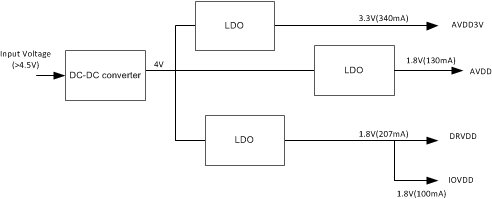
Because of the switching activities on the digital rail, it is recommended to provide the 1.8-V digital and analog supplies from separate sources. Both IOVDD and DRVDD may be supplied from a common source and a ferrite bead is recommended to separate these two supply rails. An example power supply scheme suitable for the ADS42JB46 is shown in Figure 89. In this example supply scheme, AVDD3V, AVDD, DRVDD and IOVDD are supplied from LDOs. To improve on the efficiency of the power supply scheme and to minimize heat dissipation, it is recommended that a DC-DC converter (or switcher) is used before the LDOs if the input voltage is greater than 4.5 V.
 Figure 89. Example Power Supply Scheme