ZHCSN79 September 2021 ADS131B02-Q1
PRODUCTION DATA
- 1 特性
- 2 应用
- 3 说明
- 4 Revision History
- 5 Pin Configuration and Functions
- 6 Specifications
- 7 Parameter Measurement Information
-
8 Detailed Description
- 8.1 Overview
- 8.2 Functional Block Diagram
- 8.3 Feature Description
- 8.4 Device Functional Modes
- 8.5
Programming
- 8.5.1
Serial Interface
- 8.5.1.1 Chip Select (CS)
- 8.5.1.2 Serial Data Clock (SCLK)
- 8.5.1.3 Serial Data Input (DIN)
- 8.5.1.4 Serial Data Output (DOUT)
- 8.5.1.5 Data Ready (DRDY)
- 8.5.1.6 SPI Communication Frames
- 8.5.1.7 SPI Communication Words
- 8.5.1.8 Short SPI Frames
- 8.5.1.9 Communication Cyclic Redundancy Check (CRC)
- 8.5.1.10 SPI Timeout
- 8.5.2 ADC Conversion Data Format
- 8.5.3 Commands
- 8.5.4 Collecting Data for the First Time or After a Pause in Data Collection
- 8.5.1
Serial Interface
- 8.6 Register Map
- 9 Application and Implementation
- 10Power Supply Recommendations
- 11Layout
- 12Device and Documentation Support
- 13Mechanical, Packaging, and Orderable Information
7.1 Noise Measurements
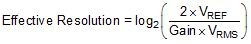
Adjust the data rate and gain to optimize the ADS131B02-Q1 noise performance. When averaging is increased by reducing the data rate, noise drops correspondingly. Table 7-1 summarizes the ADS131B02-Q1 noise performance using the 1.2-V internal reference and a 3.3-V analog power supply. The data are representative of typical noise performance at TA = 25°C when fMCLK = 8.192 MHz. The modulator clock frequency fMOD = fMCLK / 2. The data shown are typical input-referred noise results with the analog inputs shorted together and taking an average of multiple readings across all channels. A minimum 1 second of consecutive readings are used to calculate the RMS noise for each reading. Table 7-2 shows the effective resolution calculated from the noise data. Equation 1 calculates effective resolution. In each case, VREF corresponds to the internal 1.2-V reference. In global-chop mode, noise is improved by a factor of √2.
The noise performance scales with the oversampling rate (OSR) and gain settings, but is independent from the configured power mode. Thus, the device exhibits the same noise performance in different power modes when selecting the same OSR and gain settings. However, the data rate at the OSR settings scales based on the main clock frequency for the different power modes.
| OSR | DATA RATE (kSPS), fMCLK = 8.192 MHz |
GAIN | |||||||
|---|---|---|---|---|---|---|---|---|---|
| 1 | 2 | 4 | 8 | 16 | 32 | 64 | 128 | ||
| 16384 | 0.25 | 1.78 | 1.59 | 1.58 | 0.44 | 0.43 | 0.42 | 0.42 | 0.42 |
| 8192 | 0.5 | 2.51 | 2.19 | 2.07 | 0.60 | 0.59 | 0.58 | 0.58 | 0.58 |
| 4096 | 1 | 3.41 | 2.97 | 2.84 | 0.82 | 0.81 | 0.80 | 0.80 | 0.80 |
| 2048 | 2 | 4.54 | 3.96 | 3.76 | 1.07 | 1.06 | 1.05 | 1.05 | 1.05 |
| 1024 | 4 | 5.42 | 4.74 | 4.52 | 1.29 | 1.28 | 1.27 | 1.27 | 1.27 |
| 512 | 8 | 8.15 | 6.91 | 6.50 | 1.82 | 1.81 | 1.80 | 1.80 | 1.80 |
| 256 | 16 | 13.02 | 10.33 | 9.37 | 2.61 | 2.56 | 2.53 | 2.53 | 2.53 |
| 128 | 32 | 23.12 | 16.45 | 13.64 | 4.02 | 3.73 | 3.63 | 3.63 | 3.63 |
| OSR | DATA RATE (kSPS), fMCLK = 8.192 MHz |
GAIN | |||||||
|---|---|---|---|---|---|---|---|---|---|
| 1 | 2 | 4 | 8 | 16 | 32 | 64 | 128 | ||
| 16384 | 0.25 | 20.4 | 19.5 | 18.5 | 19.4 | 18.4 | 17.4 | 16.4 | 15.4 |
| 8192 | 0.5 | 19.9 | 19.1 | 18.1 | 18.9 | 18.0 | 17.0 | 16.0 | 15.0 |
| 4096 | 1 | 19.4 | 18.6 | 17.7 | 18.5 | 17.5 | 16.5 | 15.5 | 14.5 |
| 2048 | 2 | 19.0 | 18.2 | 17.3 | 18.1 | 17.1 | 16.1 | 15.1 | 14.1 |
| 1024 | 4 | 18.8 | 17.9 | 17.0 | 17.8 | 16.8 | 15.8 | 14.8 | 13.8 |
| 512 | 8 | 18.2 | 17.4 | 16.5 | 17.3 | 16.3 | 15.3 | 14.3 | 13.3 |
| 256 | 16 | 17.5 | 16.8 | 16.0 | 16.8 | 15.8 | 14.9 | 13.9 | 12.9 |
| 128 | 32 | 16.7 | 16.2 | 15.4 | 16.2 | 15.3 | 14.3 | 13.3 | 12.3 |