ZHCSN79 September   2021 ADS131B02-Q1

PRODUCTION DATA  

  1. 特性
  2. 应用
  3. 说明
  4. Revision History
  5. Pin Configuration and Functions
  6. Specifications
    1. 6.1 Absolute Maximum Ratings
    2. 6.2 ESD Ratings
    3. 6.3 Recommended Operating Conditions
    4. 6.4 Thermal Information
    5. 6.5 Electrical Characteristics
    6. 6.6 Timing Requirements
    7. 6.7 Switching Characteristics
    8. 6.8 Timing Diagrams
    9. 6.9 Typical Characteristics
  7. Parameter Measurement Information
    1. 7.1 Noise Measurements
  8. Detailed Description
    1. 8.1 Overview
    2. 8.2 Functional Block Diagram
    3. 8.3 Feature Description
      1. 8.3.1  Input ESD Protection Circuitry
      2. 8.3.2  Input Multiplexer
      3. 8.3.3  Programmable Gain Amplifier (PGA)
      4. 8.3.4  Voltage Reference
      5. 8.3.5  Internal Test Signals
      6. 8.3.6  Clocking
        1. 8.3.6.1 External Clock Using CLKIN Pin
        2. 8.3.6.2 Internal Oscillator
      7. 8.3.7  ΔΣ Modulator
      8. 8.3.8  Digital Filter
        1. 8.3.8.1 Digital Filter Implementation
          1. 8.3.8.1.1 Fast-Settling Filter
          2. 8.3.8.1.2 SINC3 and SINC3 + SINC1 Filter
        2. 8.3.8.2 Digital Filter Characteristic
      9. 8.3.9  Calibration Registers
      10. 8.3.10 Register Map CRC
    4. 8.4 Device Functional Modes
      1. 8.4.1 Power-Up and Reset
        1. 8.4.1.1 Power-On Reset
        2. 8.4.1.2 SYNC/RESET Pin
        3. 8.4.1.3 RESET Command
      2. 8.4.2 Fast Start-Up Behavior
      3. 8.4.3 Conversion Modes
        1. 8.4.3.1 Continuous-Conversion Mode
        2. 8.4.3.2 Global-Chop Mode
      4. 8.4.4 Power Modes
      5. 8.4.5 Standby Mode
      6. 8.4.6 Synchronization
    5. 8.5 Programming
      1. 8.5.1 Serial Interface
        1. 8.5.1.1  Chip Select (CS)
        2. 8.5.1.2  Serial Data Clock (SCLK)
        3. 8.5.1.3  Serial Data Input (DIN)
        4. 8.5.1.4  Serial Data Output (DOUT)
        5. 8.5.1.5  Data Ready (DRDY)
        6. 8.5.1.6  SPI Communication Frames
        7. 8.5.1.7  SPI Communication Words
        8. 8.5.1.8  Short SPI Frames
        9. 8.5.1.9  Communication Cyclic Redundancy Check (CRC)
        10. 8.5.1.10 SPI Timeout
      2. 8.5.2 ADC Conversion Data Format
      3. 8.5.3 Commands
        1. 8.5.3.1 NULL (0000 0000 0000 0000)
        2. 8.5.3.2 RESET (0000 0000 0001 0001)
        3. 8.5.3.3 STANDBY (0000 0000 0010 0010)
        4. 8.5.3.4 WAKEUP (0000 0000 0011 0011)
        5. 8.5.3.5 LOCK (0000 0101 0101 0101)
        6. 8.5.3.6 UNLOCK (0000 0110 0110 0110)
        7. 8.5.3.7 RREG (101a aaaa annn nnnn)
          1. 8.5.3.7.1 Reading a Single Register
          2. 8.5.3.7.2 Reading Multiple Registers
        8. 8.5.3.8 WREG (011a aaaa annn nnnn)
      4. 8.5.4 Collecting Data for the First Time or After a Pause in Data Collection
    6. 8.6 Register Map
  9. Application and Implementation
    1. 9.1 Application Information
      1. 9.1.1 Troubleshooting
      2. 9.1.2 Unused Inputs and Outputs
      3. 9.1.3 Antialias Filter
      4. 9.1.4 Minimum Interface Connections
      5. 9.1.5 Multiple Device Configuration
    2. 9.2 Typical Application
      1. 9.2.1 Design Requirements
      2. 9.2.2 Detailed Design Procedure
        1. 9.2.2.1 Current Shunt Measurement
        2. 9.2.2.2 Battery Pack Voltage Measurement
      3. 9.2.3 Application Curves
  10. 10Power Supply Recommendations
    1. 10.1 CAP Pin Capacitor Requirement
    2. 10.2 Power-Supply Sequencing
    3. 10.3 Power-Supply Decoupling
  11. 11Layout
    1. 11.1 Layout Guidelines
    2. 11.2 Layout Example
  12. 12Device and Documentation Support
    1. 12.1 Receiving Notification of Documentation Updates
    2. 12.2 支持资源
    3. 12.3 Trademarks
    4. 12.4 Electrostatic Discharge Caution
    5. 12.5 术语表
  13. 13Mechanical, Packaging, and Orderable Information

封装选项

机械数据 (封装 | 引脚)
散热焊盘机械数据 (封装 | 引脚)
订购信息

Antialias Filter

An analog low-pass filter is required in front of each of the ADC channel inputs to prevent out-of-band noise and interferers from coupling into the band of interest. Because the ADS131B02-Q1 is a delta-sigma ADC, the integrated digital filter provides substantial attenuation for frequencies outside of the band of interest up to the frequencies adjacent to fMOD. Therefore, a single-order RC filter with a cutoff frequency set at least two decades below the modulator frequency provides sufficient antialiasing protection in the vast majority of applications. Figure 9-1 shows a typical RC filter that yields a cutoff frequency of fC = 39.8 kHz, which is generally a good starting point for a design that uses fMOD = 4.096 MHz.

Applications that only need to measure dc signals can use much lower filter-cutoff frequencies by increasing the resistor or capacitor values. Larger resistor values have the added benefit of limiting the current into the ADC inputs in case of an overvoltage event.
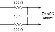
GUID-20201207-CA0I-T4P0-MS5F-L82MS21MSDFC-low.gif Figure 9-1 Antialias Filter Example