ZHCSF11B April 2016 – September 2016 ADS127L01
PRODUCTION DATA.
- 1 特性
- 2 应用
- 3 说明
- 4 修订历史记录
- 5 Pin Configuration and Functions
-
6 Specifications
- 6.1 Absolute Maximum Ratings
- 6.2 ESD Ratings
- 6.3 Recommended Operating Conditions
- 6.4 Thermal Information
- 6.5 Electrical Characteristics
- 6.6 Timing Requirements: Serial Interface
- 6.7 Switching Characteristics: Serial Interface Mode
- 6.8 Timing Requirements: Frame-Sync Master Mode
- 6.9 Switching Characteristics: Frame-Sync Master Mode
- 6.10 Timing Requirements: Frame-Sync Slave Mode
- 6.11 Switching Characteristics: Frame-Sync Slave Mode
- 6.12 Typical Characteristics
- 7 Parameter Measurement information
-
8 Detailed Description
- 8.1 Overview
- 8.2 Functional Block Diagram
- 8.3 Feature Description
- 8.4 Device Functional Modes
- 8.5
Programming
- 8.5.1 Serial Peripheral Interface (SPI) Programming
- 8.5.2
Frame-Sync Programming
- 8.5.2.1
Frame-Sync Master Mode
- 8.5.2.1.1 Chip Select (CS) in Frame-Sync Master Mode
- 8.5.2.1.2 Serial Clock (SCLK) in Frame-Sync Master Mode
- 8.5.2.1.3 Frame-Sync (DRDY/FSYNC) in Frame-Sync Master Mode
- 8.5.2.1.4 Data Input (DIN) in Frame-Sync Master Mode
- 8.5.2.1.5 Data Output (DOUT) in Frame-Sync Master Mode
- 8.5.2.1.6 Daisy-Chain Input (DAISYIN) in Frame-Sync Master Mode
- 8.5.2.2
Frame-Sync Slave Mode
- 8.5.2.2.1 Chip Select (CS) in Frame-Sync Slave Mode
- 8.5.2.2.2 Serial Clock (SCLK) in Frame-Sync Slave Mode
- 8.5.2.2.3 Frame-Sync (DRDY/FSYNC) in Frame-Sync Slave Mode
- 8.5.2.2.4 Data Input (DIN) in Frame-Sync Slave Mode
- 8.5.2.2.5 Data Output (DOUT) in Frame-Sync Slave Mode
- 8.5.2.2.6 Daisy-Chain Input (DAISYIN) in Frame-Sync Slave Mode
- 8.5.2.1
Frame-Sync Master Mode
- 8.5.3 Data Format
- 8.5.4 Status Word
- 8.5.5 Cyclic Redundancy Check (CRC)
- 8.6
Register Maps
- 8.6.1 ID: ID Control Register (address = 00h) [reset = x3h]
- 8.6.2 CONFIG: ADC Configuration Register (address = 01h) [reset = 00h]
- 8.6.3 OFC0: System Offset Calibration Register 0 (address = 02h) [reset = 00h]
- 8.6.4 OFC1: System Offset Calibration Register 1 (address = 03h) [reset = 00h]
- 8.6.5 OFC2: System Offset Calibration Register 2 (address = 04h) [reset = 00h]
- 8.6.6 FSC0: System Gain Calibration Register 0 (address = 05h) [reset = 00h]
- 8.6.7 FSC1: System Gain Calibration Register 1 (address = 06h) [reset = 80h]
- 8.6.8 MODE: Mode Settings (address = 07h) [reset = xxh]
- 9 Application and Implementation
- 10Power Supply Recommendations
- 11Layout
- 12器件和文档支持
- 13机械、封装和可订购信息
6 Specifications
6.1 Absolute Maximum Ratings(1)
| MIN | MAX | UNIT | ||
|---|---|---|---|---|
| Voltage | AVDD to AGND | –0.3 | 4.0 | V |
| DVDD to DGND | –0.3 | 4.0 | ||
| LVDD to AGND | –0.3 | 2.0 | ||
| AGND to DGND | –0.3 | 0.3 | ||
| REFP to AGND | –0.3 | AVDD + 0.3 | ||
| REFN to AGND | –0.3 | AVDD + 0.3 | ||
| Analog input | AGND – 0.3 | AVDD + 0.3 | ||
| Digital input | DGND – 0.3 | DVDD + 0.3 | ||
| Current | Input, continuous, any pin except power supply pins (2) | –10 | 10 | mA |
| Temperature | Operating ambient, TA | –40 | 125 | °C |
| Junction, TJ | 150 | |||
| Storage, Tstg | –60 | 150 | ||
(1) Stresses beyond those listed under Absolute Maximum Ratings may cause permanent damage to the device. These are stress ratings only, which do not imply functional operation of the device at these or any other conditions beyond those indicated under Recommended Operating Conditions. Exposure to absolute-maximum-rated conditions for extended periods may affect device reliability.
(2) Input pins are diode-clamped to the power-supply rails. Limit the input current to 10 mA or less if the analog input voltage exceeds AVDD + 0.3 V or is less than AGND – 0.3 V, or if the digital input voltage exceeds DVDD + 0.3 V or is less than DGND – 0.3 V.
6.2 ESD Ratings
| VALUE | UNIT | |||
|---|---|---|---|---|
| V(ESD) | Electrostatic discharge | Human-body model (HBM), per ANSI/ESDA/JEDEC JS-001(1) | ±2000 | V |
| Charged-device model (CDM), per JEDEC specification JESD22-C101(2) | ±1000 | |||
(1) JEDEC document JEP155 states that 500-V HBM allows safe manufacturing with a standard ESD control process.
(2) JEDEC document JEP157 states that 250-V CDM allows safe manufacturing with a standard ESD control process.
6.3 Recommended Operating Conditions
over operating ambient temperature range (unless otherwise noted)| MIN | NOM | MAX | UNIT | |||
|---|---|---|---|---|---|---|
| POWER SUPPLY | ||||||
| AVDD | Analog power supply | 2.7 | 3.0 | 3.6 | V | |
| LVDD | Low voltage analog supply | INTLDO = 1 | 1.7 | 1.8 | 1.9 | V |
| DVDD | Digital supply | 1.7 | 1.8 | 3.6 | V | |
| ANALOG INPUTS | ||||||
| VIN | Differential input voltage | VIN = (VAINP – VAINN) | –VREF | VREF | V | |
| VAINP, VAINN | Absolute input voltage | AINP or AINN to AGND | AGND | AVDD | V | |
| VCM | Common-mode input voltage | VCM = (VAINP + VAINN) / 2 | AVDD / 2 | V | ||
| VOLTAGE REFERENCE INPUTS | ||||||
| VREFN | Negative reference input | AGND – 0.1 | AGND | AGND + 1.0 | V | |
| VREFP | Positive reference input | VREFN + 0.5 | 2.5 | AVDD | V | |
| VREF | Reference input voltage | VREF = VREFP – VREFN | 0.5 | 2.5 | 3.0 | V |
| EXTERNAL CLOCK SOURCE | ||||||
| fCLK | Master clock rate(1) | HR mode | 0.1 | 16.384 | 17.6 | MHz |
| LP mode | 0.1 | 8.192 | 8.8 | |||
| VLP mode | 0.1 | 4.096 | 4.4 | |||
| DIGITAL INPUTS | ||||||
| Input voltage | DGND | DVDD | V | |||
| TEMPERATURE RANGE | ||||||
| TA | Operating ambient temperature | –40 | 125 | °C | ||
(1) To meet maximum speed conditions, fCLK duty cycle must be 49% < duty cycle < 51%.
6.4 Thermal Information
| THERMAL METRIC(1) | ADS127L01 | UNIT | |
|---|---|---|---|
| PBS (TQFP) | |||
| 32 PINS | |||
| RθJA | Junction-to-ambient thermal resistance | 73.4 | °C/W |
| RθJC(top) | Junction-to-case (top) thermal resistance | 15.9 | °C/W |
| RθJB | Junction-to-board thermal resistance | 26.7 | °C/W |
| ψJT | Junction-to-top characterization parameter | 0.4 | °C/W |
| ψJB | Junction-to-board characterization parameter | 26.5 | °C/W |
| RθJC(bot) | Junction-to-case (bottom) thermal resistance | N/A | °C/W |
(1) For more information about traditional and new thermal metrics, see the Semiconductor and IC Package Thermal Metrics application report.
6.5 Electrical Characteristics
Minimum and maximum specifications apply from TA = –40°C to +125°C. Typical specifications are at TA = 25°C.All specifications are at AVDD = 3 V, LVDD = 1.8 V (external), DVDD = 1.8 V, VREF = 2.5 V, INTLDO = 1, FILTER[1:0] = 01 (WB2), and fCLK = 16.384 MHz for HR mode, 8.192 MHz for LP mode, or 4.096 MHz for VLP mode (unless otherwise noted)
| PARAMETER | TEST CONDITIONS | MIN | TYP | MAX | UNIT | |||
|---|---|---|---|---|---|---|---|---|
| ANALOG INPUTS | ||||||||
| Differential input impedance | HR mode, fCLK = 16.384 MHz | 5 | kΩ | |||||
| LP mode, fCLK = 8.192 MHz | 11 | |||||||
| VLP mode, fCLK = 4.096 MHz | 23 | |||||||
| DC PERFORMANCE | ||||||||
| Resolution | No missing codes | 24 | Bits | |||||
| fDATA | Data rate | HR mode | Wideband filters | 512, 256, 128, 64 | kSPS | |||
| Low-latency filter | 512, 128, 32, 8 | |||||||
| LP mode | Wideband filters | 256, 128, 64, 32 | ||||||
| Low-latency filter | 256, 64, 16, 4 | |||||||
| VLP mode | Wideband filters | 128, 64, 32, 16 | ||||||
| Low-latency filter | 128, 32, 8, 2 | |||||||
| INL | Integral nonlinearity(1) | HR mode | VCM = AVDD / 2 | 2.5 | 10 | ppm | ||
| LP mode | VCM = AVDD / 2 | 1 | 5 | |||||
| VLP mode | VCM = AVDD / 2 | 1 | 5 | |||||
| Offset error | ±0.1 | mV | ||||||
| Offset drift | 1.5 | 3.0 | μV/°C | |||||
| Gain error | 0.2 | %FSR | ||||||
| Gain calibration accuracy | 0.003% | |||||||
| Gain drift | HR mode | 0.8 | 3 | ppm/°C | ||||
| LP mode | 0.4 | 2.5 | ||||||
| VLP mode | 0.2 | 2 | ||||||
| Noise(2) | HR mode | WB2, OSR 32 | 10.6 | μVRMS | ||||
| WB2, OSR 64 | 7.3 | 10.1 | ||||||
| WB2, OSR 128 | 5.1 | 7.2 | ||||||
| WB2, OSR 256 | 3.6 | 5.2 | ||||||
| CMRR | Common-mode rejection ratio | fCM = 60 Hz | 95 | dB | ||||
| PSRR | Power-supply rejection ratio | fPS = 60 Hz | AVDD | 90 | dB | |||
| DVDD | 85 | |||||||
| LVDD | 80 | |||||||
| AC PERFORMANCE | ||||||||
| SNR | Signal-to-noise ratio(2)(3) | WB2, OSR 32 | 104.4 | dB | ||||
| WB2, OSR 64 | 104.9 | 107.8 | ||||||
| WB2, OSR 128 | 107.9 | 110.9 | ||||||
| WB2, OSR 256 | 110.6 | 113.9 | ||||||
| WB2, OSR 32, VREF = 3 V | 105.8 | |||||||
| WB2, OSR 64, VREF = 3 V | 109.3 | |||||||
| WB2, OSR 128, VREF = 3 V | 112 | |||||||
| WB2, OSR 256, VREF = 3 V | 115.5 | |||||||
| THD | Total harmonic distortion(4) | HR mode, fIN = 4 kHz, VIN = –0.5 dBFS | –113 | dB | ||||
| LP mode, fIN = 4 kHz, VIN = –0.5 dBFS | –126 | |||||||
| VLP mode, fIN = 4 kHz, VIN = –0.5 dBFS | –129 | |||||||
| SFDR | Spurious-free dynamic range | HR mode | –115 | dB | ||||
| LP mode | –130 | |||||||
| VLP mode | –130 | |||||||
| DIGITAL FILTER RESPONSE: WIDEBAND | ||||||||
| Bandwidth | See Table 1 | |||||||
| Pass-band ripple | ±0.000032 | dB | ||||||
| Transition band | FILTER[1:0] = 00 (WB1) | (0.45 to 0.55) × fDATA | Hz | |||||
| FILTER[1:0] = 01 (WB2) | (0.40 to 0.50) × fDATA | |||||||
| Stop-band attenuation | 116 | dB | ||||||
| Group delay | 42 / fDATA | s | ||||||
| Settling time | Complete settling | 84 / fDATA | s | |||||
| DIGITAL FILTER RESPONSE: LOW-LATENCY | ||||||||
| Bandwidth | See Table 2 | |||||||
| Group delay | See Low-Latency Filter section | |||||||
| Settling time | See Low-Latency Filter section | |||||||
| VOLTAGE REFERENCE INPUTS | ||||||||
| Reference input impedance | HR mode | 2.2 | kΩ | |||||
| LP mode | 3.2 | |||||||
| VLP mode | 4 | |||||||
| SYSTEM MONITORS | ||||||||
| Input over-range detect accuracy | ±100 | mV | ||||||
| DIGITAL INPUT/OUTPUT (DVDD = 1.7 V to 3.6 V) | ||||||||
| VIH | High-level input voltage | 0.7 DVDD | DVDD | V | ||||
| VIL | Low-level input voltage | DGND | 0.3 DVDD | V | ||||
| VOH | High-level output voltage | IOH = 2 mA | 0.8 DVDD | DVDD | V | |||
| VOL | Low-level output voltage | IOL = 2 mA | DGND | 0.2 DVDD | V | |||
| IH | Input leakage, high | IH = 3.6 V | –10 | 10 | μA | |||
| IL | Input leakage, low | IL = DGND | –10 | 10 | μA | |||
| POWER SUPPLY | ||||||||
| Power-down current | AVDD | INTLDO = 0 | 8 | μA | ||||
| INTLDO = 1 | 2 | |||||||
| DVDD | 0.6 | |||||||
| LVDD, INTLDO = 1 | 0.6 | |||||||
| IAVDD | AVDD current | HR mode | 1.3 | 1.6 | mA | |||
| LP mode | 0.8 | 1.0 | ||||||
| VLP mode | 0.4 | 0.6 | ||||||
| ILVDD | LVDD current(5) (6) | HR mode | 9.3 | 11 | mA | |||
| LP mode | 4.6 | 5.5 | ||||||
| VLP mode | 2.3 | 2.8 | ||||||
| IDVDD | DVDD current(2) | HR mode | OSR 128 | 2.8 | 3.4 | mA | ||
| LP mode | OSR 128 | 1.5 | 1.8 | |||||
| VLP mode | OSR 128 | 0.8 | 1.1 | |||||
| PD | Power dissipation | HR mode, OSR 128, AVDD = 3.0 V, DVDD = 1.8 V |
INTLDO = 1, LVDD = 1.8 V, |
25.7 | 30.8 | mW | ||
| INTLDO = 0 | 36.8 | 44.2 | ||||||
| LP mode, OSR 128, AVDD = 3.0 V, DVDD = 1.8 V |
INTLDO = 1, LVDD = 1.8 V, |
13.4 | 16.1 | |||||
| INTLDO = 0 | 18.9 | 22.7 | ||||||
| VLP mode, OSR 128, AVDD = 3.0 V, DVDD = 1.8 V |
INTLDO = 1, LVDD = 1.8 V, |
6.8 | 8.2 | |||||
| INTLDO = 0 | 9.5 | 11.4 | ||||||
(1) Best fit method.
(2) For all Wideband filter configurations, see Table 1. For all Low-latency filter configurations, see Table 2.
(3) Minimum SNR is ensured by the limit of the dc noise specification.
(4) THD includes the first nine harmonics of the input signal.
(5) LVDD current sourced from AVDD when the internal LDO is used (INTLDO = 0).
(6) LVDD current scales with fCLK; see Figure 47.
6.6 Timing Requirements: Serial Interface
over operating ambient temperature range (unless otherwise noted)| 2.8 V < DVDD ≤ 3.6 V | 1.7 V ≤ DVDD ≤ 2.8 V | UNIT | |||||||
|---|---|---|---|---|---|---|---|---|---|
| MIN | TYP | MAX | MIN | TYP | MAX | ||||
| tc(CLK) | Master clock period | HR mode | 57 | 10,000 | 57 | 10,000 | ns | ||
| LP mode | 114 | 10,000 | 114 | 10,000 | |||||
| VLP mode | 227 | 10,000 | 227 | 10,000 | |||||
| tw(CP) | Pulse duration, Master clock high or low | HR mode | 28 | 5,000 | 28 | 5,000 | ns | ||
| LP mode | 56 | 5,000 | 56 | 5,000 | |||||
| VLP mode | 112 | 5,000 | 112 | 5,000 | |||||
| td(CSSC) | Delay time, CS falling edge to first SCLK rising edge(1) | 8 | 12 | ns | |||||
| tc(SC) | SCLK period | 40 | 6250 | 50 | 6250 | ns | |||
| tw(SCHL) | Pulse duration, SCLK high or low | 20 | 25 | ns | |||||
| tsu(DI) | Setup time, DIN valid before SCLK falling edge | 6 | 9 | ns | |||||
| th(DI) | Hold time, DIN valid after SCLK falling edge | 8 | 9 | ns | |||||
| tw(CSH) | Pulse duration, CS high | 6 | 6 | tCLK | |||||
| td(SCCS) | Delay time, final SCLK falling edge to CS rising edge | 2 | 2 | tCLK | |||||
| td(DECODE) | Delay time, command decode time | 4 | 4 | tCLK | |||||
| SPI timeout(2) | TOUT_DEL = 0 | 216 | 216 | tCLK | |||||
| TOUT_DEL = 1 | 214 | 214 | tCLK | ||||||
| tsu(DCI) | Setup time, DAISYIN valid before SCLK falling edge | 5 | 8 | ns | |||||
| th(DCI) | Hold time, DAISYIN valid after SCLK falling edge | 20 | 25 | ns | |||||
(1) CS can be tied low permanently in case the serial bus is not shared with any other device.
(2) See the SPI Timeout section for more information.
6.7 Switching Characteristics: Serial Interface Mode
over operating ambient temperature range (unless otherwise noted)| 2.8 V < DVDD ≤ 3.6 V | 1.7 V ≤ DVDD ≤ 2.8 V | UNIT | |||||||
|---|---|---|---|---|---|---|---|---|---|
| MIN | TYP | MAX | MIN | TYP | MAX | ||||
| tp(CSDO) | Propagation delay time, CS falling edge to DOUT driven |
12 | 18 | ns | |||||
| tp(SCDO) | Propagation delay time, SCLK rising edge to valid new DOUT |
15 | 21 | ns | |||||
| tv(DO) | Valid time, SCLK falling edge to DOUT invalid | 18 | tSCLK / 2 | 20 | tSCLK / 2 | ns | |||
| tp(CSDOZ) | Propagation delay time, CS rising edge to DOUT high impedance |
20 | 20 | ns | |||||
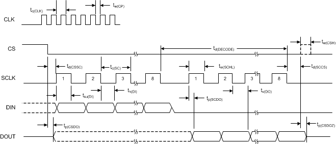
NOINDENT:
NOTE: SPI settings are CPOL = 0 and CPHA = 1.6.8 Timing Requirements: Frame-Sync Master Mode
over operating ambient temperature range and DVDD = 1.7 V to 3.6 V (unless otherwise noted)| 1.7 V ≤ DVDD ≤ 3.6 V | UNIT | |||||
|---|---|---|---|---|---|---|
| MIN | TYP | MAX | ||||
| tc(CLK) | Master clock period | HR mode | 57 | 10,000 | ns | |
| LP mode | 114 | 10,000 | ||||
| VLP mode | 227 | 10,000 | ||||
| tw(CP) | Pulse duration, Master clock high or low | HR mode | 28 | 5,000 | ns | |
| LP mode | 56 | 5,000 | ||||
| VLP mode | 112 | 5,000 | ||||
6.9 Switching Characteristics: Frame-Sync Master Mode
over operating free-air temperature range (unless otherwise noted)| 2.8 V < DVDD ≤ 3.6 V | 1.7 V ≤ DVDD ≤ 2.8 V | UNIT | |||||||
|---|---|---|---|---|---|---|---|---|---|
| MIN | TYP | MAX | MIN | TYP | MAX | ||||
| td(CSC) | Delay time, CLK rising edge to SCLK falling edge | 15 | 15 | ns | |||||
| tc(FRAME) | Frame period | 1 / fDATA | 1 / fDATA | s | |||||
| tw(FP) | Pulse duration, FSYNC high or low | 1 / (2fDATA) | 1 / (2fDATA) | s | |||||
| td(FSSC) | Delay time, FSYNC rising edge to SCLK falling edge | 6 | 8 | ns | |||||
| tc(SC) | SCLK period | 1 / (32fDATA) | 1 / (32fDATA) | s | |||||
| tw(SCHL) | Pulse duration, SCLK high or low | 1 / (64fDATA) | 1 / (64fDATA) | s | |||||
| tv(DO) | Valid time, SCLK rising edge to DOUT invalid | 25 | 25 | ns | |||||
| tp(SCDO) | Propagation delay time, SCLK falling edge to DOUT driven |
15 | 17 | ns | |||||
| tp(FSDO) | Propagation delay time, FSYNC rising edge to DOUT MSB valid |
12 | 15 | ns | |||||
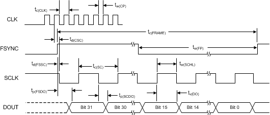 Figure 3. Frame-Sync Interface Timing Master Mode
6.10 Timing Requirements: Frame-Sync Slave Mode
over operating ambient temperature range (unless otherwise noted)| 2.8 V < DVDD ≤ 3.6 V | 1.7 V ≤ DVDD ≤ 2.8 V | UNIT | |||||||
|---|---|---|---|---|---|---|---|---|---|
| MIN | TYP | MAX | MIN | TYP | MAX | ||||
| tc(CLK) | Master clock period | HR mode | 57 | 10,000 | 57 | 10,000 | ns | ||
| LP mode | 114 | 10,000 | 114 | 10,000 | |||||
| VLP mode | 227 | 10,000 | 227 | 10,000 | |||||
| tw(CP) | Pulse duration, Master clock high or low | HR mode | 28 | 5,000 | 28 | 5,000 | ns | ||
| LP mode | 56 | 5,000 | 56 | 5,000 | |||||
| VLP mode | 112 | 5,000 | 112 | 5,000 | |||||
| td(CSC) | Delay time, CLK rising edge to SCLK falling edge | 2 | 2 | ns | |||||
| tc(FRAME) | Frame period | 1 / fDATA | 1 / fDATA | s | |||||
| tw(FP) | Pulse durration, FSYNC high or low | 2 | 2 | tSCLK | |||||
| td(FSSC) | Delay time, FSYNC rising edge to SCLK falling edge | 6 | 6 | ns | |||||
| td(SCFS) | Delay time, SCLK falling edge to FSYNC rising edge | 2 | 2 | ns | |||||
| tc(SC) | SCLK period | 40 | 56 | ns | |||||
| tw(SCHL) | Pulse duration, SCLK high or low | 20 | 28 | ns | |||||
| DAISY-CHAIN TIMING | |||||||||
| tsu(DCI) | Setup time, DAISYIN valid before SCLK rising edge | 8 | 8 | ns | |||||
| th(DCI) | Hold time, DAISYIN valid after SCLK rising edge | 25 | 31 | ns | |||||
6.11 Switching Characteristics: Frame-Sync Slave Mode
over operating ambient temperature range (unless otherwise noted)| 2.8 V < DVDD ≤ 3.6 V | 1.7 V ≤ DVDD ≤ 2.8 V | UNIT | |||||||
|---|---|---|---|---|---|---|---|---|---|
| MIN | TYP | MAX | MIN | TYP | MAX | ||||
| tv(DO) | Valid time, SCLK rising edge to DOUT invalid | 17 | 25 | ns | |||||
| tp(SCDO) | Propagation delay time, SCLK falling edge to valid new DOUT |
22 | 22 | ns | |||||
| tp(FSDO) | Propagation delay time, FSYNC rising edge to DOUT MSB valid |
15 | 22 | 25 | 32 | ns | |||
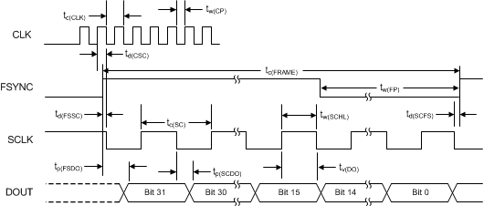 Figure 4. Frame-Sync Interface Timing Slave Mode
 Figure 5. Frame-Sync Interface Slave Daisy-Chain Timing
6.12 Typical Characteristics
At TA = 25°C, AVDD = 3.3 V, and external VREF = 2.5 V (unless otherwise noted)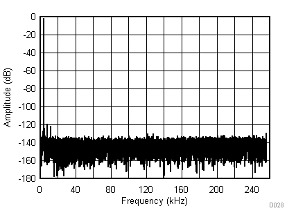
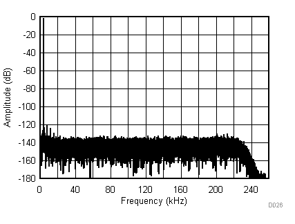
| fIN = 4 kHz, VIN = –0.5 dBFS, HR mode, WB1, 512 kSPS, 32768 samples |
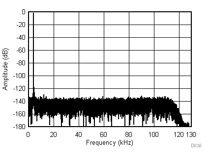
| fIN = 4 kHz, VIN = –0.5 dBFS, LP mode, WB2, 256 kSPS, 32768 samples |
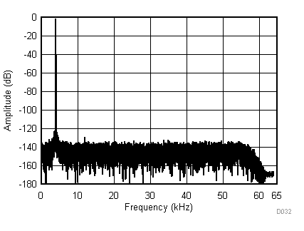
| fIN = 4 kHz, VIN = –0.5 dBFS, VLP mode, WB2, 128 kSPS, 32768 samples |
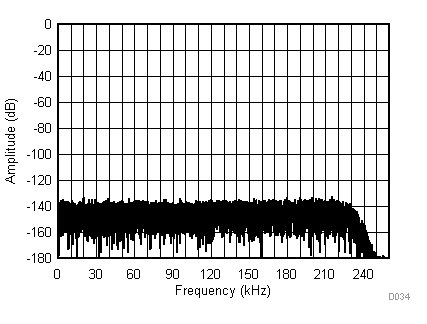
| Inputs shorted, HR mode, WB2, 512 kSPS, 32768 samples |
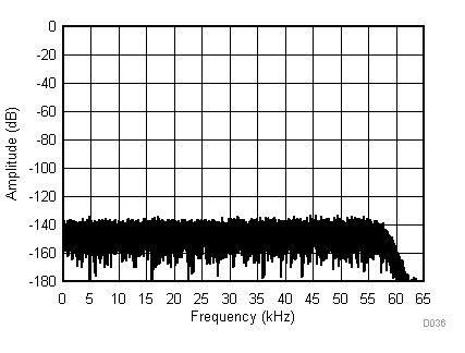
| Inputs shorted, VLP mode, WB2, 128 kSPS, 32768 samples |
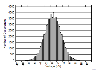
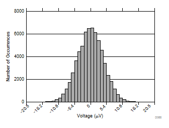
| Inputs shorted, HR mode, 65536 points |
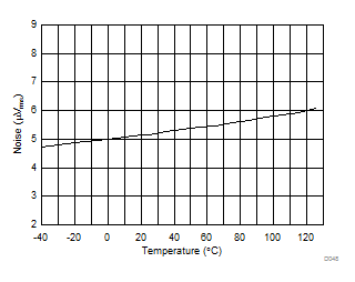
| Inputs shorted |
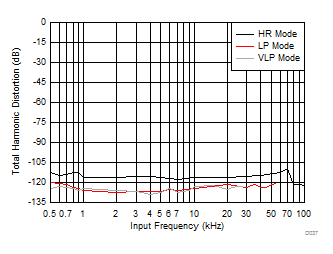
| WB2, OSR 32 |
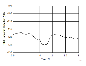
| HR mode, fIN = 4 kHz, VIN = –0.5 dBFS |
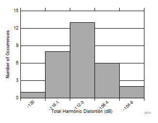
| HR mode, fIN = 4 kHz, VIN = –0.5 dBFS |
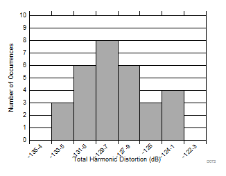
| VLP mode, fIN = 4 kHz, VIN = –0.5 dBFS |
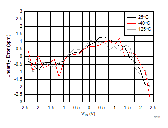
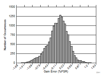
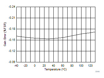
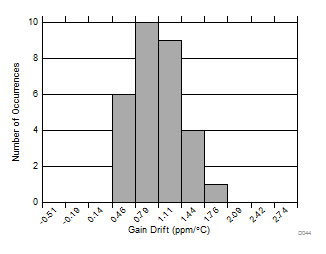
| HR mode, 30 Devices |
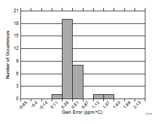
| VLP mode, 30 Devices |
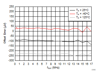
| Inputs shorted, HR mode |
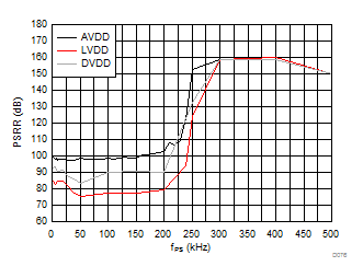
| HR mode, INTLDO = 1 |
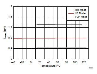
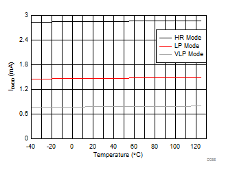
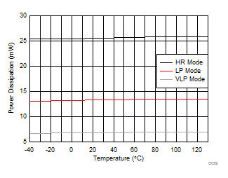
| INTLDO = 1, LVDD = 1.8 V |
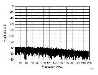
| Inputs shorted, HR mode, LL, 512 kSPS, 32768 samples |
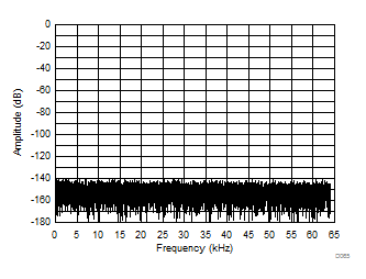
| Inputs shorted, HR mode, LL, 32 kSPS, 32768 samples |
| Inputs shorted, HR mode, LL, 512 kSPS, 32768 samples |
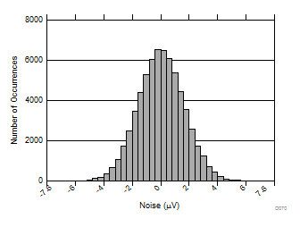
| Inputs shorted, HR mode, LL, 32 kSPS, 32768 samples |
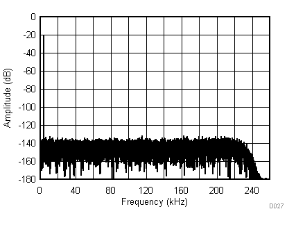
| fIN = 4 kHz, VIN = –20 dBFS, HR mode, WB2, 512 kSPS, 32768 samples |
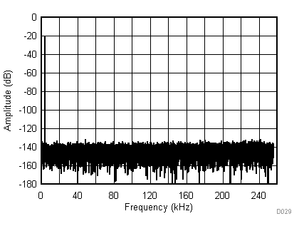
| fIN = 4 kHz, VIN = –20 dBFS, HR mode, WB1, 512 kSPS, 32768 samples |
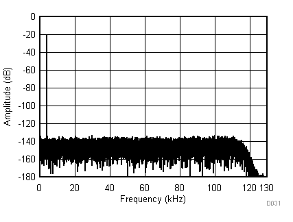
| fIN = 4 kHz, VIN = –20 dBFS, LP mode, WB2, 256 kSPS, 32768 samples |
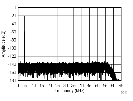
| fIN = 4 kHz, VIN = –20 dBFS, VLP mode, WB2, 128 kSPS, 32768 samples |
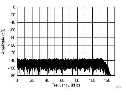
| Inputs shorted, LP mode, WB2, 256 kSPS, 32768 samples |
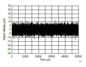
| HR mode, 0.5 seconds data collection space |
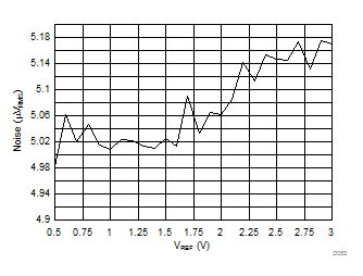
| Inputs shorted, HR mode |
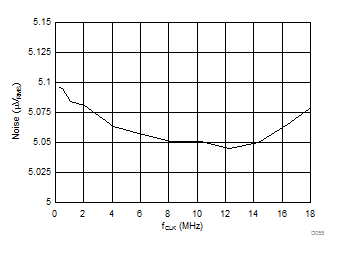
| Inputs shorted, HR mode |
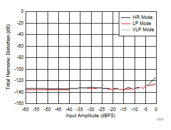
| WB2, OSR 32 |
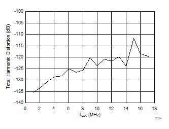
| fIN = 4 kHz, HR mode |
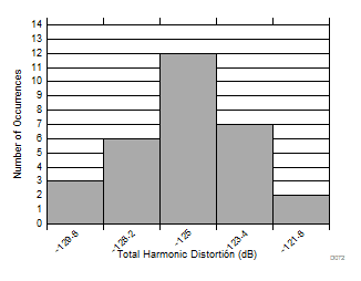
| LP mode, fIN = 4 kHz, VIN = –0.5 dBFS |
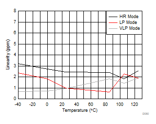
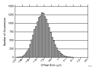
| Inputs shorted |
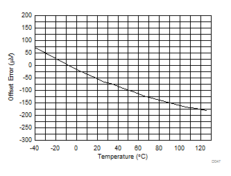
| Inputs shorted |
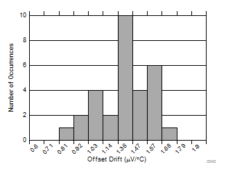
| Inputs shorted, 30 devices |
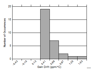
| LP mode, 30 Devices |
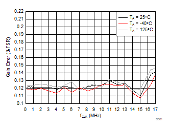
| HR mode |
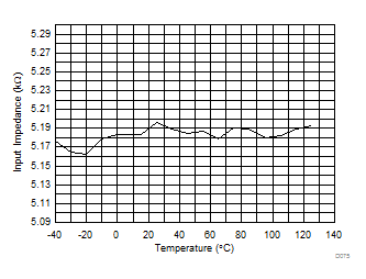
| HR mode, fCLK = 16.384 MHz |
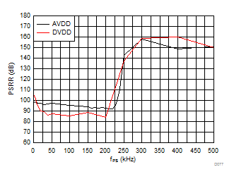
| HR mode, INTLDO = 0 |
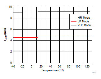
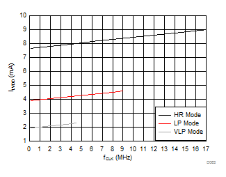
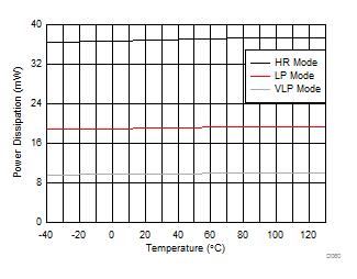
| INTLDO = 0 |

| Inputs shorted, HR mode, LL, 128 kSPS, 32768 samples |
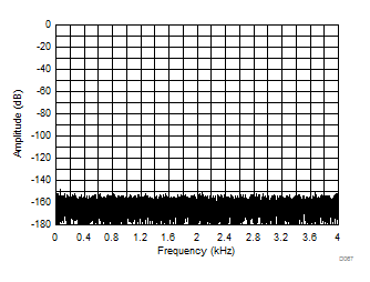
| Inputs shorted, HR mode, LL, 8 kSPS, 32768 samples |
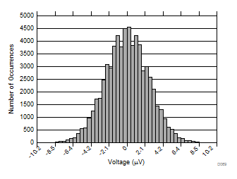
| Inputs shorted, HR mode, LL, 128 kSPS, 32768 samples |
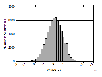
| Inputs shorted, HR mode, LL, 8 kSPS, 32768 samples |

