ZHCSF11B April 2016 – September 2016 ADS127L01
PRODUCTION DATA.
- 1 特性
- 2 应用
- 3 说明
- 4 修订历史记录
- 5 Pin Configuration and Functions
-
6 Specifications
- 6.1 Absolute Maximum Ratings
- 6.2 ESD Ratings
- 6.3 Recommended Operating Conditions
- 6.4 Thermal Information
- 6.5 Electrical Characteristics
- 6.6 Timing Requirements: Serial Interface
- 6.7 Switching Characteristics: Serial Interface Mode
- 6.8 Timing Requirements: Frame-Sync Master Mode
- 6.9 Switching Characteristics: Frame-Sync Master Mode
- 6.10 Timing Requirements: Frame-Sync Slave Mode
- 6.11 Switching Characteristics: Frame-Sync Slave Mode
- 6.12 Typical Characteristics
- 7 Parameter Measurement information
-
8 Detailed Description
- 8.1 Overview
- 8.2 Functional Block Diagram
- 8.3 Feature Description
- 8.4 Device Functional Modes
- 8.5
Programming
- 8.5.1 Serial Peripheral Interface (SPI) Programming
- 8.5.2
Frame-Sync Programming
- 8.5.2.1
Frame-Sync Master Mode
- 8.5.2.1.1 Chip Select (CS) in Frame-Sync Master Mode
- 8.5.2.1.2 Serial Clock (SCLK) in Frame-Sync Master Mode
- 8.5.2.1.3 Frame-Sync (DRDY/FSYNC) in Frame-Sync Master Mode
- 8.5.2.1.4 Data Input (DIN) in Frame-Sync Master Mode
- 8.5.2.1.5 Data Output (DOUT) in Frame-Sync Master Mode
- 8.5.2.1.6 Daisy-Chain Input (DAISYIN) in Frame-Sync Master Mode
- 8.5.2.2
Frame-Sync Slave Mode
- 8.5.2.2.1 Chip Select (CS) in Frame-Sync Slave Mode
- 8.5.2.2.2 Serial Clock (SCLK) in Frame-Sync Slave Mode
- 8.5.2.2.3 Frame-Sync (DRDY/FSYNC) in Frame-Sync Slave Mode
- 8.5.2.2.4 Data Input (DIN) in Frame-Sync Slave Mode
- 8.5.2.2.5 Data Output (DOUT) in Frame-Sync Slave Mode
- 8.5.2.2.6 Daisy-Chain Input (DAISYIN) in Frame-Sync Slave Mode
- 8.5.2.1
Frame-Sync Master Mode
- 8.5.3 Data Format
- 8.5.4 Status Word
- 8.5.5 Cyclic Redundancy Check (CRC)
- 8.6
Register Maps
- 8.6.1 ID: ID Control Register (address = 00h) [reset = x3h]
- 8.6.2 CONFIG: ADC Configuration Register (address = 01h) [reset = 00h]
- 8.6.3 OFC0: System Offset Calibration Register 0 (address = 02h) [reset = 00h]
- 8.6.4 OFC1: System Offset Calibration Register 1 (address = 03h) [reset = 00h]
- 8.6.5 OFC2: System Offset Calibration Register 2 (address = 04h) [reset = 00h]
- 8.6.6 FSC0: System Gain Calibration Register 0 (address = 05h) [reset = 00h]
- 8.6.7 FSC1: System Gain Calibration Register 1 (address = 06h) [reset = 80h]
- 8.6.8 MODE: Mode Settings (address = 07h) [reset = xxh]
- 9 Application and Implementation
- 10Power Supply Recommendations
- 11Layout
- 12器件和文档支持
- 13机械、封装和可订购信息
10 Power Supply Recommendations
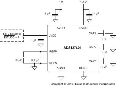
The ADS127L01 requires either two or three power supplies, depending on if the internal LDO is used to supply the LVDD analog supply. The AVDD analog supply is referenced to AGND, the LVDD analog supply is referenced to AGND, and the DVDD digital supply is referenced to DGND. The analog power supply can only be unipolar (for example, AVDD = 3.0 V, AGND = 0 V) and is independent of the digital power supply. If INTLDO = 0, the LVDD supply is internally generated using the AVDD supply. If INTLDO = 1, the internal LDO is disabled and LVDD supply must be externally supplied. The digital supply sets the digital I/O levels.
10.1 Power-Supply Sequencing
The power supplies can be sequenced in any order, but in no case must any analog or digital inputs exceed the respective analog or digital power-supply voltage limits. Bring the RESET/PWDN pin high after the analog and digital supplies are up, or bring the pin high with the DVDD supply (assuming the AVDD and LVDD supplies come up with or before DVDD). After all supplies are stabilized, wait for the td(POR) timing for the power-on-reset to complete before communicating with the device in order to allow the power-up reset process to complete.
10.2 Power-Supply Decoupling
Good power-supply decoupling is important to achieve optimum performance. AVDD, LVDD, and DVDD must be decoupled with at least a 1-µF capacitor, as shown in Figure 129. Place the bypass capacitors as close to the power-supply pins of the device as possible using low-impedance connections. Use multilayer ceramic chip capacitors (MLCCs) that offer low equivalent series resistance (ESR) and inductance (ESL) characteristics for power-supply decoupling purposes. For very sensitive systems, or for systems in harsh noise environments, avoid the use of vias for connecting the capacitors to the device pins for superior noise immunity. The use of multiple vias in parallel lowers the overall inductance and is beneficial for connections to ground planes. Connect analog and digital ground together as close to the device as possible.
 Figure 129. ADS127L01 Recommended Power-Supply Decoupling