ZHCSCV9A August 2014 – October 2014 ADS1120-Q1
PRODUCTION DATA.
- 1 特性
- 2 应用
- 3 说明
- 4 修订历史记录
- 5 Pin Configurations and Functions
- 6 Specifications
- 7 Parameter Measurement Information
-
8 Detailed Description
- 8.1 Overview
- 8.2 Functional Block Diagram
- 8.3
Feature Description
- 8.3.1 Multiplexer
- 8.3.2 Low-Noise PGA
- 8.3.3 Modulator
- 8.3.4 Digital Filter
- 8.3.5 Output Data Rate
- 8.3.6 Voltage Reference
- 8.3.7 Clock Source
- 8.3.8 Excitation Current Sources
- 8.3.9 Low-Side Power Switch
- 8.3.10 Sensor Detection
- 8.3.11 System Monitor
- 8.3.12 Offset Calibration
- 8.3.13 Power Supplies
- 8.3.14 Temperature Sensor
- 8.4 Device Functional Modes
- 8.5 Programming
- 8.6 Register Map
- 9 Application and Implementation
- 10Power-Supply Recommendations
- 11Layout
- 12器件和文档支持
- 13机械封装和可订购信息
6 Specifications
6.1 Absolute Maximum Ratings(1)
| MIN | MAX | UNIT | ||
|---|---|---|---|---|
| AVDD to AVSS | –0.3 | 7 | V | |
| DVDD to DGND | –0.3 | 7 | V | |
| AVSS to DGND | –2.8 | 0.3 | V | |
| Analog input voltage | AVSS – 0.3 | AVDD + 0.3 | V | |
| Digital input voltage | DGND – 0.3 | DVDD + 0.3 | V | |
| Input current, continuous, any terminal except power supply terminals | –10 | 10 | mA | |
| Junction temperature, TJ | –40 | 150 | °C | |
(1) Stresses beyond those listed under Absolute Maximum Ratings may cause permanent damage to the device. These are stress ratings only, which do not imply functional operation of the device at these or any other conditions beyond those indicated under Recommended Operating Conditions. Exposure to absolute-maximum-rated conditions for extended periods may affect device reliability.
6.2 Handling Ratings
| MIN | MAX | UNIT | ||||
|---|---|---|---|---|---|---|
| Tstg | Storage temperature range | –60 | 150 | °C | ||
| V(ESD) | Electrostatic discharge | Human body model (HBM), per AEC Q100-002(1) | –2000 | 2000 | V | |
| Charged device model (CDM), per AEC Q100-011 | Corner pins (1, 8, 9, and 16) |
–750 | 750 | V | ||
| Other pins | –500 | 500 | V | |||
(1) AEC Q100-002 indicates HBM stressing is done in accordance with the ANSI/ESDA/JEDEC JS-001 specification.
6.3 Recommended Operating Conditions
over operating ambient temperature range (unless otherwise noted)| MIN | NOM | MAX | UNIT | |||
|---|---|---|---|---|---|---|
| POWER SUPPLY | ||||||
| Unipolar analog power supply | AVDD to AVSS | 2.3 | 5.5 | V | ||
| AVSS to DGND | –0.1 | 0 | 0.1 | V | ||
| Bipolar analog power supply | AVDD to DGND | 2.3 | 2.5 | 2.75 | V | |
| AVSS to DGND | –2.75 | –2.5 | –2.3 | V | ||
| Digital power supply | DVDD to DGND | 2.3 | 5.5 | V | ||
| ANALOG INPUTS(1) | ||||||
| VIN | Differential input voltage | VIN = V(AINP) – V(AINN)(2) | –Vref / Gain | Vref / Gain | V | |
| V(AINx) | Absolute input voltage | PGA disabled, gain = 1 to 4 | AVSS – 0.1 | AVDD + 0.1 | V | |
| PGA enabled, gain = 1 to 128 | See the Low-Noise PGA section | |||||
| VCM | Common-mode input voltage | PGA disabled, gain = 1 to 4 | AVSS – 0.1 | AVDD + 0.1 | V | |
| PGA enabled, gain = 1 to 128 | See the Low-Noise PGA section | |||||
| VOLTAGE REFERENCE INPUTS(3) | ||||||
| Vref | Differential reference input voltage | Vref = V(REFPx) – V(REFNx) | 0.75 | 2.5 | AVDD | V |
| V(REFNx) | Absolute negative reference voltage | AVSS – 0.1 | V(REFPx) – 0.75 | V | ||
| V(REFPx) | Absolute positive reference voltage | V(REFNx) + 0.75 | AVDD + 0.1 | V | ||
| EXTERNAL CLOCK SOURCE | ||||||
| f(CLK) | External clock frequency | 0.5 | 4.096 | 4.5 | MHz | |
| Duty cycle | 40% | 60% | ||||
| DIGITAL INPUTS | ||||||
| Input voltage | DGND | DVDD | V | |||
| TEMPERATURE RANGE | ||||||
| TA | Operating ambient temperature | –40 | 125 | °C | ||
(1) AINP and AINN denote the positive and negative inputs of the PGA. AINx denotes one of the four available analog inputs.
PGA disabled means the low-noise PGA is powered down and bypassed. Gains of 1, 2, and 4 are still possible in this case.
See the Bypassing the PGA section for more information.
PGA disabled means the low-noise PGA is powered down and bypassed. Gains of 1, 2, and 4 are still possible in this case.
See the Bypassing the PGA section for more information.
(2) Excluding the effects of offset and gain error.
Limited to ±[(AVDD – AVSS) – 0.4 V] / Gain, when the PGA is enabled.
Limited to ±[(AVDD – AVSS) – 0.4 V] / Gain, when the PGA is enabled.
(3) REFPx and REFNx denote one of the two available differential reference input pairs.
6.4 Thermal Information
| THERMAL METRIC(1) | TSSOP (PW) | UNIT | |
|---|---|---|---|
| 16 PINS | |||
| RθJA | Junction-to-ambient thermal resistance | 99.5 | °C/W |
| RθJC(top) | Junction-to-case (top) thermal resistance | 35.2 | |
| RθJB | Junction-to-board thermal resistance | 44.3 | |
| ψJT | Junction-to-top characterization parameter | 2.4 | |
| ψJB | Junction-to-board characterization parameter | 43.8 | |
| RθJC(bot) | Junction-to-case (bottom) thermal resistance | n/a | |
(1) For more information about traditional and new thermal metrics, see the IC Package Thermal Metrics application report, SPRA953.
6.5 Electrical Characteristics
Minimum and maximum specifications apply from TA = –40°C to +125°C. Typical specifications are at TA = 25°C.All specifications are at AVDD = 3.3 V, AVSS = 0 V, DVDD = 3.3 V, PGA enabled, DR = 20 SPS, and external Vref = 2.5 V (unless otherwise noted).(1)
| PARAMETER | TEST CONDITIONS | MIN | TYP | MAX | UNIT | ||
|---|---|---|---|---|---|---|---|
| ANALOG INPUTS | |||||||
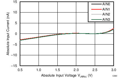
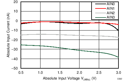
| Absolute input current | See the Typical Characteristics | ||||||
| Differential input current | See the Typical Characteristics | ||||||
| SYSTEM PERFORMANCE | |||||||
| Resolution (no missing codes) | 16 | Bits | |||||
| DR | Data rate | Normal mode | 20, 45, 90, 175, 330, 600, 1000 | SPS | |||
| Duty-cycle mode | 5, 11.25, 22.5, 44, 82.5, 150, 250 | SPS | |||||
| Turbo mode | 40, 90, 180, 350, 660, 1200, 2000 | SPS | |||||
| Noise (input-referred) | See the Noise Performance section | ||||||
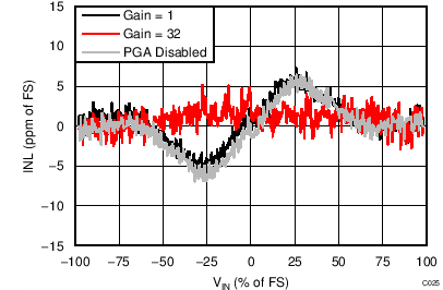
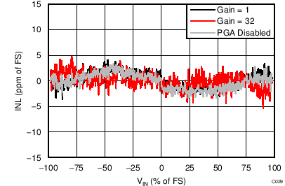
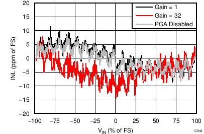
| INL | Integral nonlinearity | Gain = 1, VCM = 0.5 AVDD, best fit(2) | 8 | 20 | ppm | ||
| Gain = 2 to 128, VCM = 0.5 AVDD, best fit | 8 | ppm | |||||
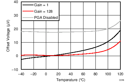
| VIO | Input offset voltage | PGA disabled, gain = 1 to 4, differential inputs |
±4 | µV | |||
| Gain = 1 to 128, differential inputs | ±4 | µV | |||||
| Offset drift | PGA disabled, gain = 1 to 4 | 0.25 | µV/°C | ||||
| Gain = 1 to 128 | 0.25 | µV/°C | |||||
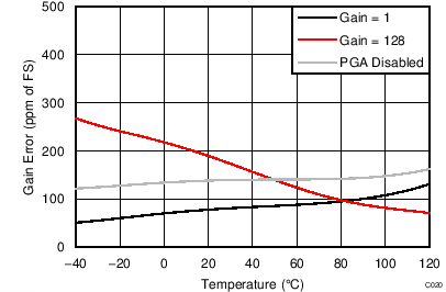
| Gain error | PGA disabled, gain = 1 to 4 | ±0.015% | |||||
| Gain = 1 to 128, TA = 25°C | –0.1% | ±0.015% | 0.1% | ||||
| Gain drift | PGA disabled, gain = 1 to 4 | 1 | ppm/°C | ||||
| Gain = 1 to 128(2) | 1 | 5 | ppm/°C | ||||
| NMRR | Normal-mode rejection ratio(2) | 50 Hz ±3%, DR = 20 SPS, external CLK, 50/60 bit = 10 | 105 | dB | |||
| 60 Hz ±3%, DR = 20 SPS, external CLK, 50/60 bit = 11 | 105 | dB | |||||
| 50 Hz or 60 Hz ±3%, DR = 20 SPS, external CLK, 50/60 bit = 01 | 90 | dB | |||||
| CMRR | Common-mode rejection ratio | At dc, gain = 1 | 90 | 105 | dB | ||
| f(CM) = 50 Hz, DR = 2000 SPS(2) | 90 | 115 | dB | ||||
| f(CM) = 60 Hz, DR = 2000 SPS(2) | 90 | 115 | dB | ||||
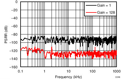
| PSRR | Power-supply rejection ratio | AVDD at dc, VCM = 0.5 AVDD, gain = 1 | 80 | 105 | dB | ||
| DVDD at dc, VCM = 0.5 AVDD, gain = 1(2) | 90 | 115 | dB | ||||
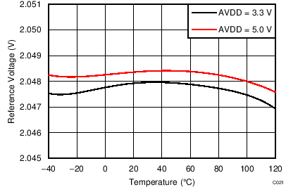
| INTERNAL VOLTAGE REFERENCE | |||||||
| Initial accuracy | TA = 25°C | 2.045 | 2.048 | 2.051 | V | ||
| Reference drift(2) | 5 | 40 | ppm/°C | ||||
| Long-term drift | 1000 hours | 110 | ppm | ||||
| VOLTAGE REFERENCE INPUTS | |||||||
| Reference input current | REFP0 = Vref, REFN0 = AVSS | ±10 | nA | ||||
| INTERNAL OSCILLATOR | |||||||
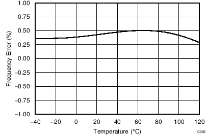
| Internal oscillator accuracy | Normal mode | –2% | ±1% | 2% | |||
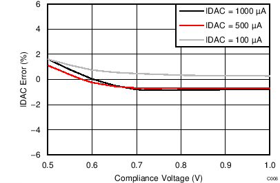
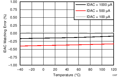
| EXCITATION CURRENT SOURCES (IDACs) | |||||||
| Current settings | 50, 100, 250, 500, 1000, 1500 | µA | |||||
| Compliance voltage | All current settings | AVDD – 0.9 | V | ||||
| Accuracy | All current settings, each IDAC | –6% | ±1% | 6% | |||
| Current match | Between IDACs | ±0.3% | |||||
| Temperature drift | Each IDAC | 50 | ppm/°C | ||||
| Temperature drift matching | Between IDACs | 10 | ppm/°C | ||||
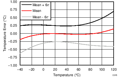
| TEMPERATURE SENSOR | |||||||
| Temperature sensor resolution | Conversion resolution | 14 | Bits | ||||
| Temperature resolution | 0.03125 | °C | |||||
| Temperature sensor accuracy | TA = 0°C to +75°C | ±0.25 | °C | ||||
| TA = –40°C to +125°C | ±0.5 | °C | |||||
| Temperature sensor accuracy vs analog supply voltage | 0.0625 | 0.25 | °C/V | ||||
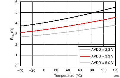
| LOW-SIDE POWER SWITCH | |||||||
| RON | On-resistance | 3.5 | Ω | ||||
| Current through switch | 30 | mA | |||||
| DIGITAL INPUT/OUTPUT | |||||||
| VIH | High-level input voltage | 0.7 DVDD | DVDD | V | |||
| VIL | Low-level input voltage | DGND | 0.3 DVDD | V | |||
| VOH | High-level output voltage | IOH = 3 mA | 0.8 DVDD | V | |||
| VOL | Low-level output voltage | IOL = 3 mA | 0.2 DVDD | V | |||
| IH | Input leakage, high | VIH = 5.5 V | –10 | 10 | µA | ||
| IL | Input leakage, low | VIL = DGND | –10 | 10 | µA | ||
| POWER-SUPPLY | |||||||
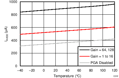
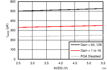
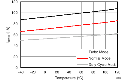
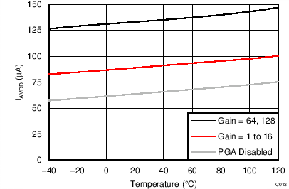
| IAVDD | Analog supply current(3) | Power-down mode | 0.1 | 3 | µA | ||
| Duty-cycle mode, PGA disabled | 65 | µA | |||||
| Normal mode, PGA disabled | 240 | µA | |||||
| Normal mode, gain = 1 to 16 | 340 | 490 | µA | ||||
| Normal mode, gain = 32 | 425 | µA | |||||
| Normal mode, gain = 64, 128 | 510 | µA | |||||
| Turbo mode, gain = 1 to 16 | 540 | µA | |||||
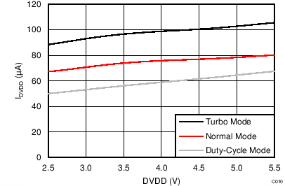
| IDVDD | Digital supply current(3) | Power-down mode | 0.3 | 5 | µA | ||
| Duty-cycle mode | 55 | µA | |||||
| Normal mode | 75 | 110 | µA | ||||
| Turbo mode | 95 | µA | |||||
| PD | Power dissipation(3) | Duty-cycle mode, PGA disabled | 0.4 | mW | |||
| Normal mode, gain = 1 to 16 | 1.4 | mW | |||||
| Turbo mode, gain = 1 to 16 | 2.1 | mW | |||||
(1) PGA disabled means the low-noise PGA is powered down and bypassed. Gains of 1, 2, and 4 are still possible in this case.
See the Bypassing the PGA section for more information.
See the Bypassing the PGA section for more information.
(2) Minimum and maximum values are ensured by design and characterization data.
(3) Internal voltage reference selected, internal oscillator enabled, both IDACs turned off.
6.6 SPI Timing Requirements
over operating ambient temperature range, DVDD = 2.3 V to 5.5 V (unless otherwise noted)| MIN | MAX | UNIT | ||
|---|---|---|---|---|
| td(CSSC) | Delay time, CS falling edge to first SCLK rising edge | 50 | ns | |
| td(SCCS) | Delay time, final SCLK falling edge to CS rising edge | 25 | ns | |
| tw(CSH) | Pulse duration, CS high | 50 | ns | |
| tc(SC) | SCLK period(1) | 150 | ns | |
| tw(SCH) | Pulse duration, SCLK high(1) | 60 | ns | |
| tw(SCL) | Pulse duration, SCLK low(1) | 60 | ns | |
| tsu(DI) | Setup time, DIN valid before SCLK falling edge | 50 | ns | |
| th(DI) | Hold time, DIN valid after SCLK falling edge | 25 | ns | |
(1) If a complete command is not sent within 13955 · t(MOD) (normal mode, duty-cycle mode) or 27910 · t(MOD) (turbo mode), the serial interface resets and the next SCLK pulse starts a new communication cycle.
t(MOD) = 1 / f(MOD). Modulator frequency (f(MOD)) is 256 kHz in normal and duty-cycle mode and 512 kHz in turbo mode, when using the internal oscillator or an external 4.096-MHz clock.
t(MOD) = 1 / f(MOD). Modulator frequency (f(MOD)) is 256 kHz in normal and duty-cycle mode and 512 kHz in turbo mode, when using the internal oscillator or an external 4.096-MHz clock.
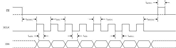
NOTE: Single-byte communication is shown. Actual communication may be multiple bytes.
Figure 1. Serial Interface Timing Requirements
6.7 SPI Switching Characteristics
over operating ambient temperature range, DVDD = 2.3 V to 5.5 V (unless otherwise noted)| PARAMETER | TEST CONDITIONS | MIN | TYP | MAX | UNIT | |
|---|---|---|---|---|---|---|
| tp(CSDO) | Propagation delay time, CS falling edge to DOUT driven |
DOUT load = 20 pF || 10 kΩ to DGND | 50 | ns | ||
| tp(SCDO) | Propagation delay time, SCLK rising edge to valid new DOUT |
DOUT load = 20 pF || 10 kΩ to DGND | 0 | 50 | ns | |
| tp(CSDOZ) | Propagation delay time, CS rising edge to DOUT high impedance |
DOUT load = 20 pF || 10 kΩ to DGND | 50 | ns | ||
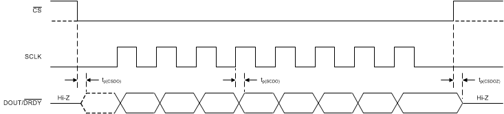
NOTE: Single-byte communication is shown. Actual communication may be multiple bytes.
Figure 2. Serial Interface Switching Characteristics
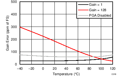
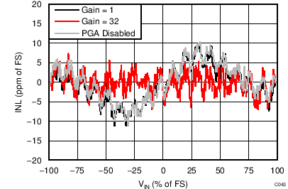
6.8 Typical Characteristics
At TA = 25°C, AVDD = 3.3 V, AVSS = 0 V, and PGA enabled using external Vref = 2.5 V (unless otherwise noted).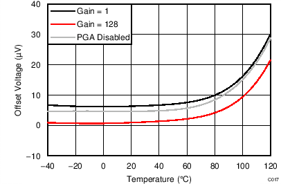
| AVDD = 3.3 V |
| AVDD = 3.3 V |
| AVDD = 3.3 V, external 2.5-V reference, normal mode |
Differential Input Signal
| AVDD = 3.3 V, internal reference, normal mode |
Differential Input Signal
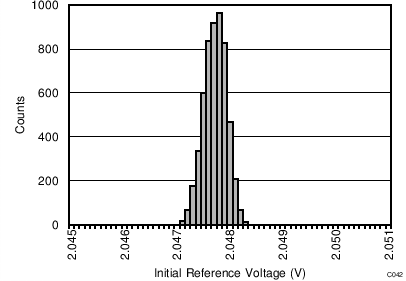
| TA = 25°C, data from 5490 devices |
| DVDD = 3.3 V, normal mode |
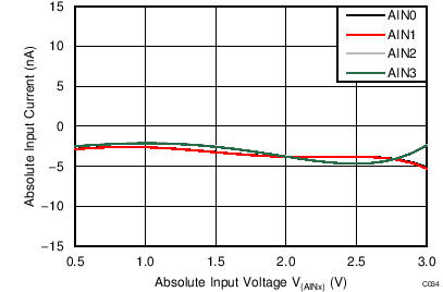
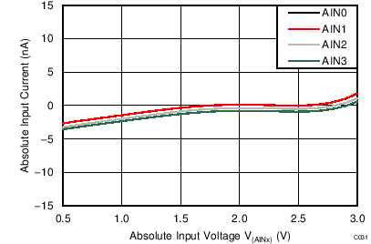
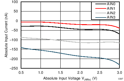
| AVDD = 3.3 V, PGA enabled, TA = –40°C |
Absolute Input Voltage
| AVDD = 3.3 V, PGA enabled, TA = 85°C |
Absolute Input Voltage
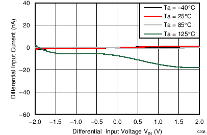
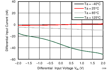
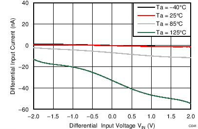
| AVDD = 3.3 V, PGA enabled, AINP = AIN0, AINN = AIN1 |
Differential Input Voltage
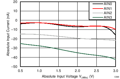
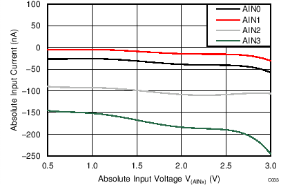
| AVDD = 3.3 V, PGA disabled, TA = –40°C |
Absolute Input Voltage
| AVDD = 3.3 V, PGA disabled, TA = 85°C |
Absolute Input Voltage
| AVDD = 3.3 V, PGA disabled, AINP = AIN0, AINN = AIN1 |
Differential Input Voltage
| AVDD = 3.3 V, internal reference, turbo mode |
| Normal mode, internal reference |
| DVDD = 3.3 V |
| AVDD = 5.0 V |
| AVDD = 5.0 V |
| AVDD = 5.0 V, external 2.5-V reference, normal mode |
Differential Input Signal
| AVDD = 5.0 V, internal reference, normal mode |
Differential Input Signal
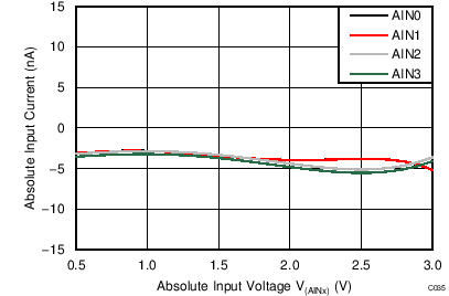
| AVDD = 3.3 V, PGA enabled, TA = 25°C |
Absolute Input Voltage
| AVDD = 3.3 V, PGA enabled, TA = 125°C |
Absolute Input Voltage
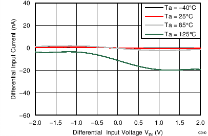
| AVDD = 3.3 V, PGA enabled, AINP = AIN3, AINN = AIN2 |
Differential Input Voltage
| AVDD = 3.3 V, PGA disabled, TA = 25°C |
Absolute Input Voltage
| AVDD = 3.3 V, PGA disabled, TA = 125°C |
Absolute Input Voltage
| AVDD = 3.3 V, PGA disabled, AINP = AIN3, AINN = AIN2 |
Differential Input Voltage
| AVDD = 3.3 V, internal reference, normal mode |
| AVDD = 3.3 V, internal reference, duty-cycle mode |